

Question: Please can someone help solve this!!! STUDENT NUMBER IS 101143850 (a) Assuming that your student ID is hexadecimal, convert its two least significant digits to
Please can someone help solve this!!!
STUDENT NUMBER IS 101143850
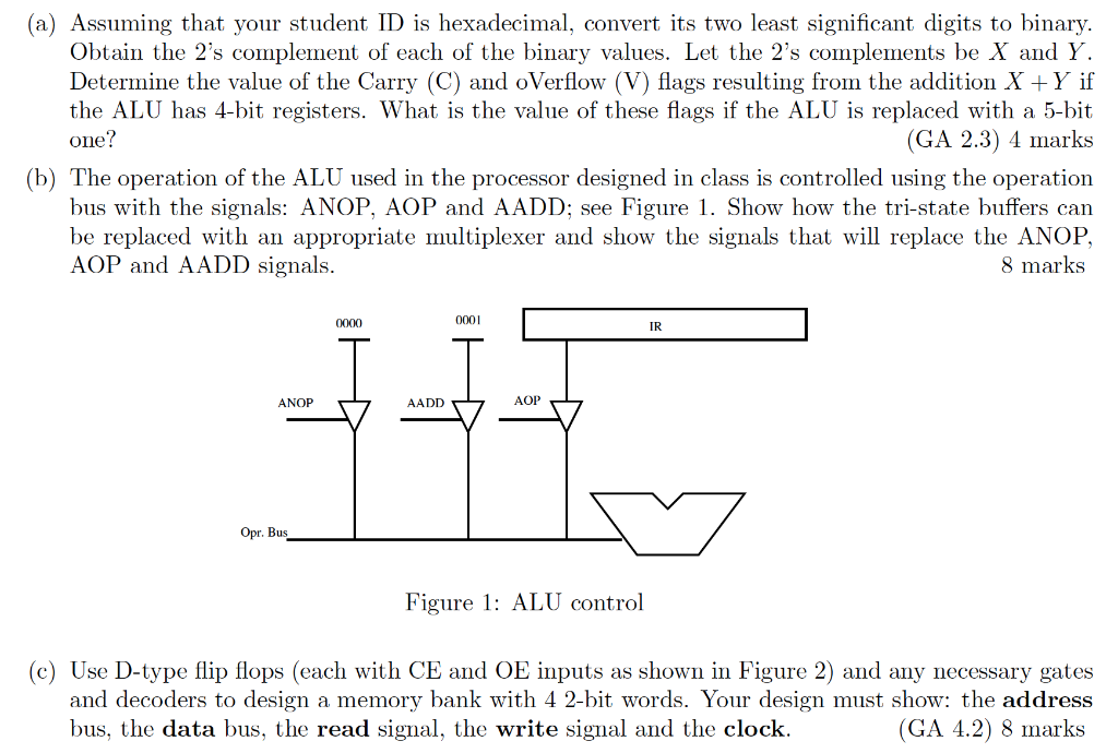
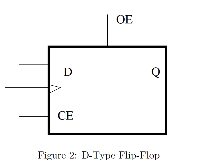
(a) Assuming that your student ID is hexadecimal, convert its two least significant digits to binary. Obtain the 2's complement of each of the binary values. Let the 2's complements be X and Y. Determine the value of the Carry (C) and oVerflow (V) flags resulting from the addition X+Y if the ALU has 4-bit registers. What is the value of these flags if the ALU is replaced with a 5-bit one? (GA 2.3) 4 marks (b) The operation of the ALU used in the processor designed in class is controlled using the operation bus with the signals: ANOP, AOP and AADD; see Figure 1. Show how the tri-state buffers can be replaced with an appropriate multiplexer and show the signals that will replace the ANOP, AOP and AADD signals. 8 marks 0000 0001 IR ANOP AADD AOP Opr. Bus Figure 1: ALU control (c) Use D-type flip flops (each with CE and OE inputs as shown in Figure 2) and any necessary gates and decoders to design a memory bank with 4 2-bit words. Your design must show: the address bus, the data bus, the read signal, the write signal and the clock. (GA 4.2) 8 marks OE D Q CE Figure 2: D-Type Flip-Flop (a) Assuming that your student ID is hexadecimal, convert its two least significant digits to binary. Obtain the 2's complement of each of the binary values. Let the 2's complements be X and Y. Determine the value of the Carry (C) and oVerflow (V) flags resulting from the addition X+Y if the ALU has 4-bit registers. What is the value of these flags if the ALU is replaced with a 5-bit one? (GA 2.3) 4 marks (b) The operation of the ALU used in the processor designed in class is controlled using the operation bus with the signals: ANOP, AOP and AADD; see Figure 1. Show how the tri-state buffers can be replaced with an appropriate multiplexer and show the signals that will replace the ANOP, AOP and AADD signals. 8 marks 0000 0001 IR ANOP AADD AOP Opr. Bus Figure 1: ALU control (c) Use D-type flip flops (each with CE and OE inputs as shown in Figure 2) and any necessary gates and decoders to design a memory bank with 4 2-bit words. Your design must show: the address bus, the data bus, the read signal, the write signal and the clock. (GA 4.2) 8 marks OE D Q CE Figure 2: D-Type Flip-Flop
Step by Step Solution
There are 3 Steps involved in it

Get step-by-step solutions from verified subject matter experts