

Question: Please explain the logic behind it. Data Bus (8 bits) CPU Address Bus (16 bits) AD-A13 AO-A13 DO-D7 DO-D7 AO RAM 1 AO RAM 2

Please explain the logic behind it.
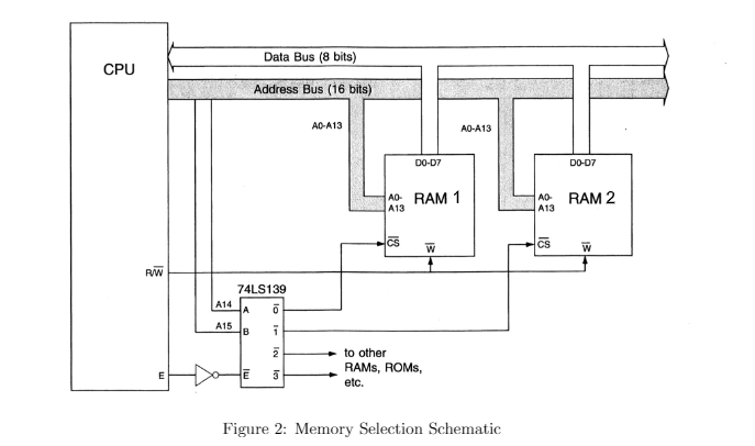
Data Bus (8 bits) CPU Address Bus (16 bits) AD-A13 AO-A13 DO-D7 DO-D7 AO RAM 1 AO RAM 2 A13 A13 CS w CS RW 74LS139 A14 lo A15 I B Tyle to other RAMS, ROMs, etc. E Figure 2: Memory Selection Schematic Referring to Figure 2, assume that the address on the address bus is 0x3AFF. Which RAM chip (if any) would be activated? What address in the activated chip would be read or written
Step by Step Solution
There are 3 Steps involved in it
1 Expert Approved Answer
Step: 1 Unlock

Question Has Been Solved by an Expert!
Get step-by-step solutions from verified subject matter experts
Step: 2 Unlock
Step: 3 Unlock