Question: Please follow steps table is provided. can be simulated. Lab 3 Karnaugh Maps Due Date: Sunday of Week 6 by 11:55 PM In this lab
Please follow steps table is provided. can be simulated.
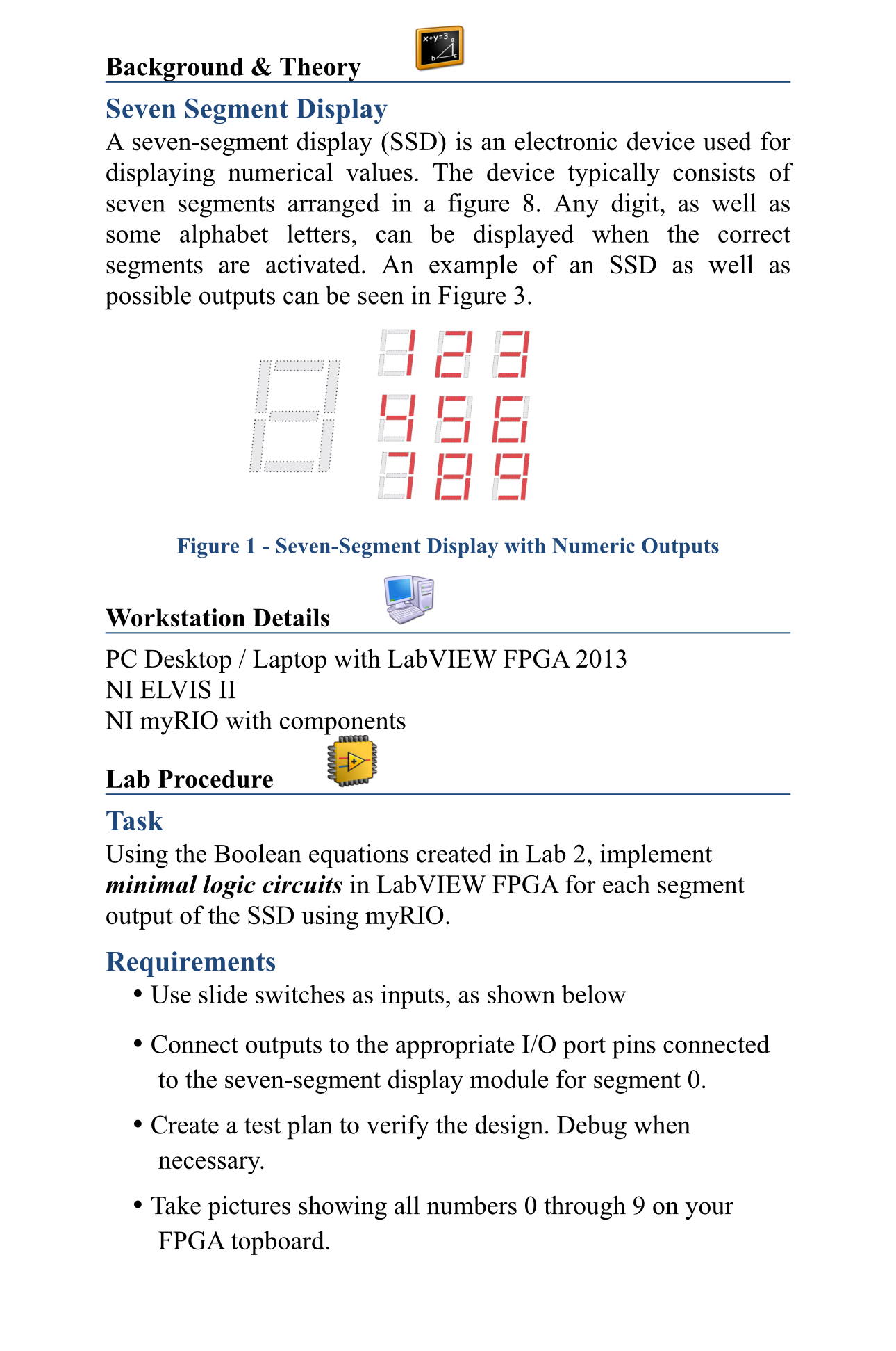
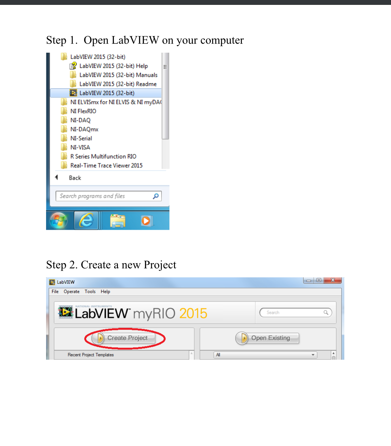
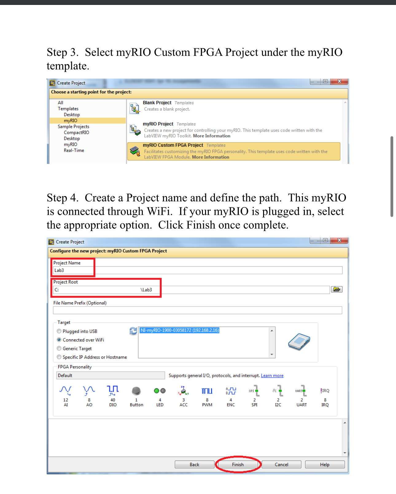
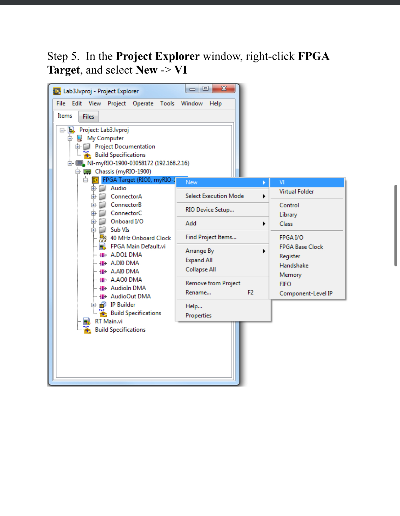
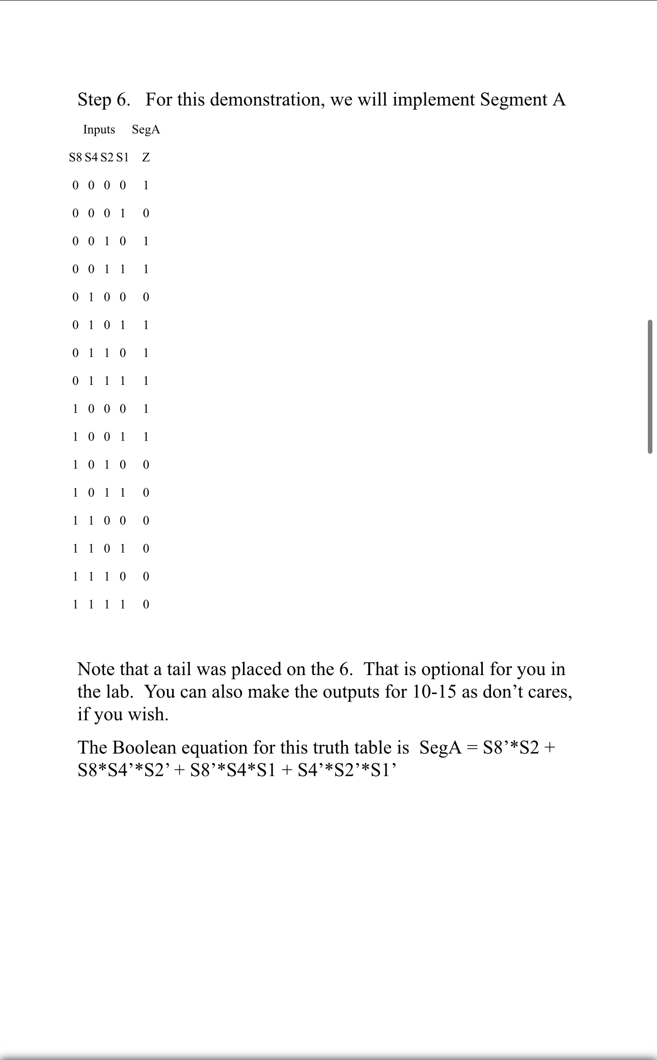
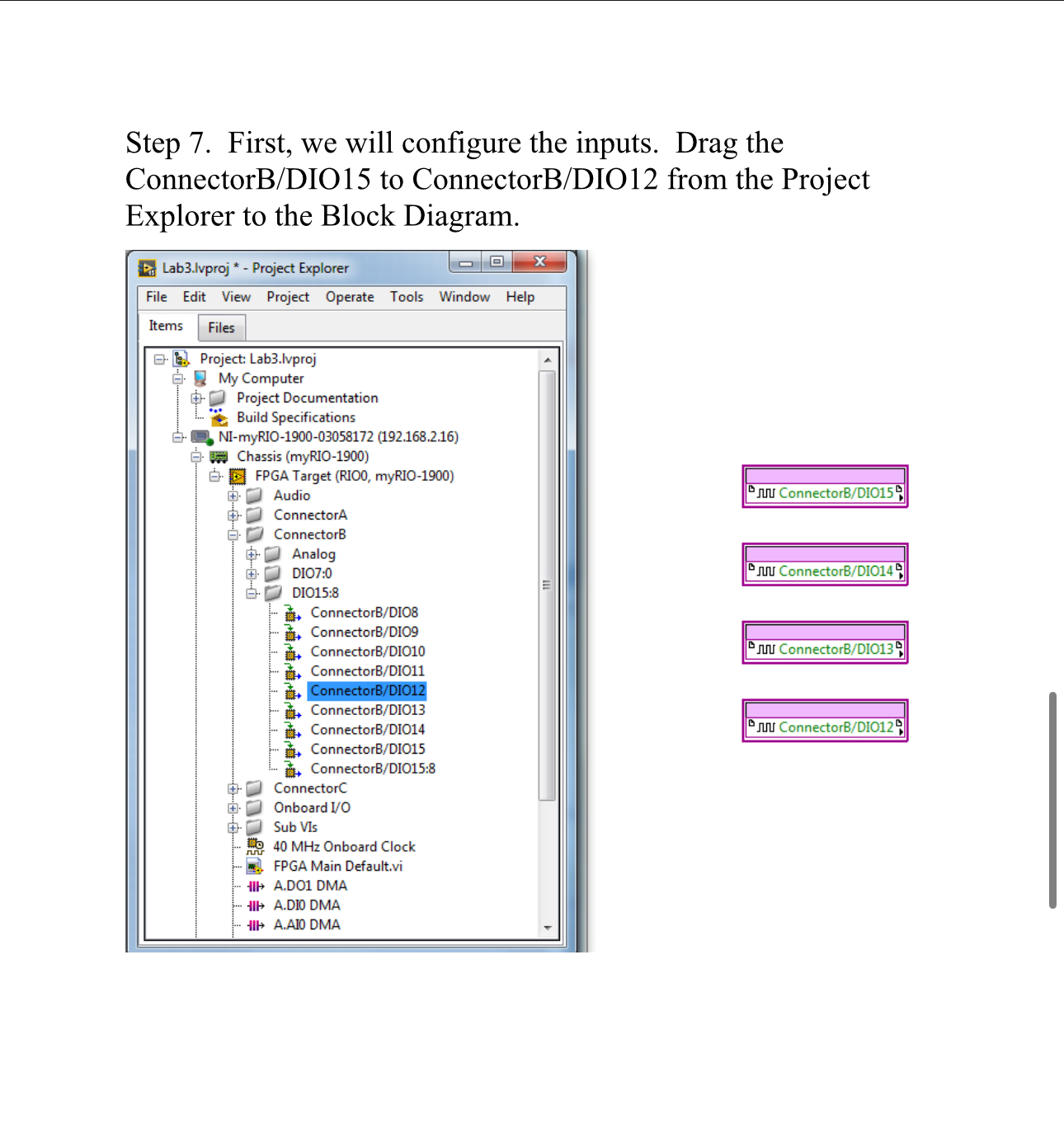
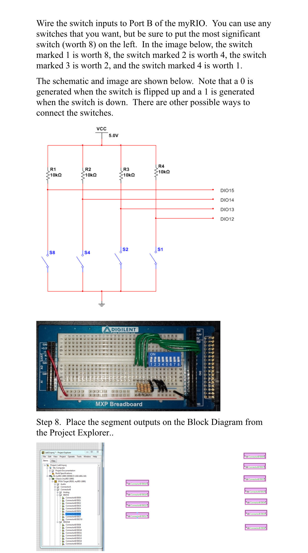
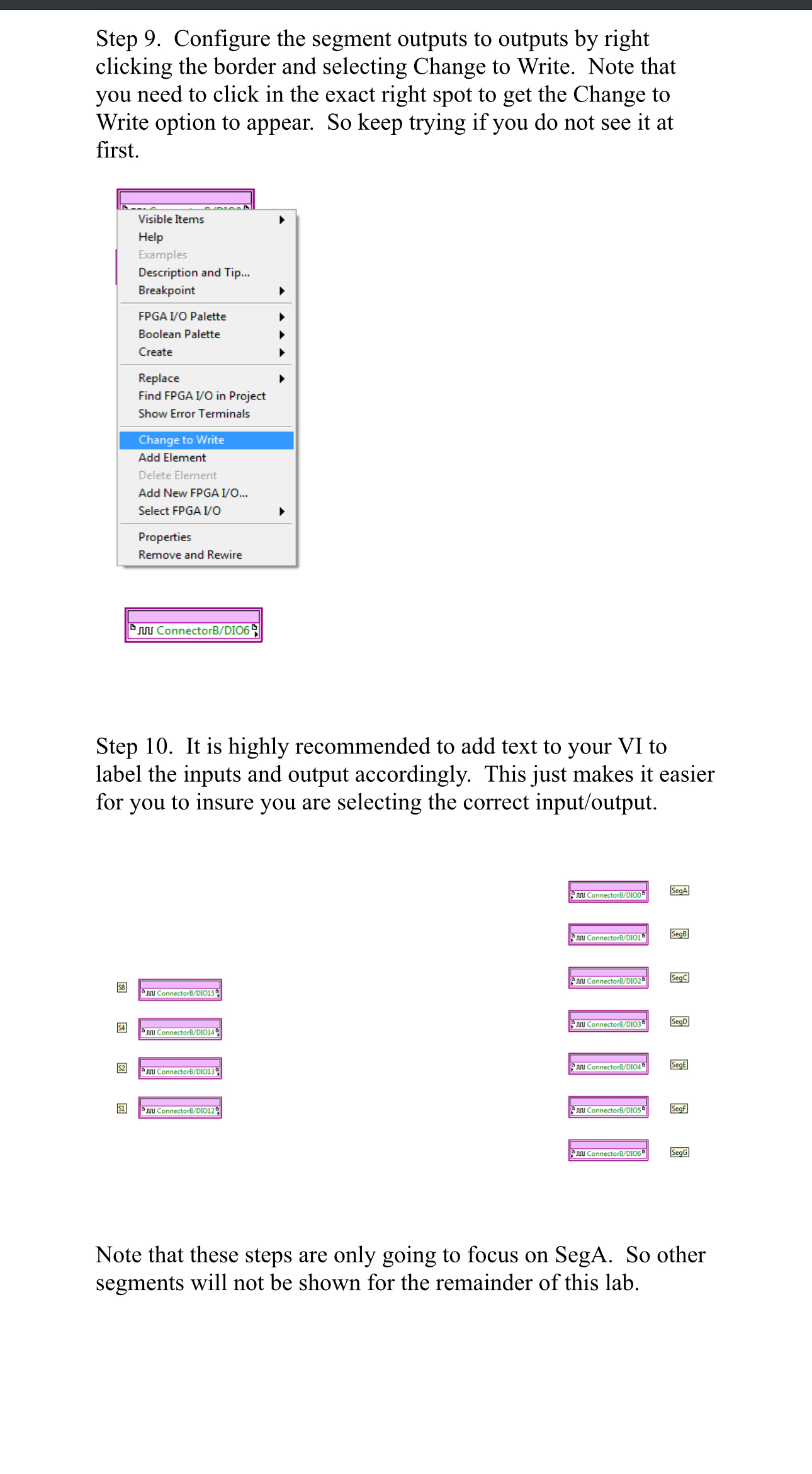
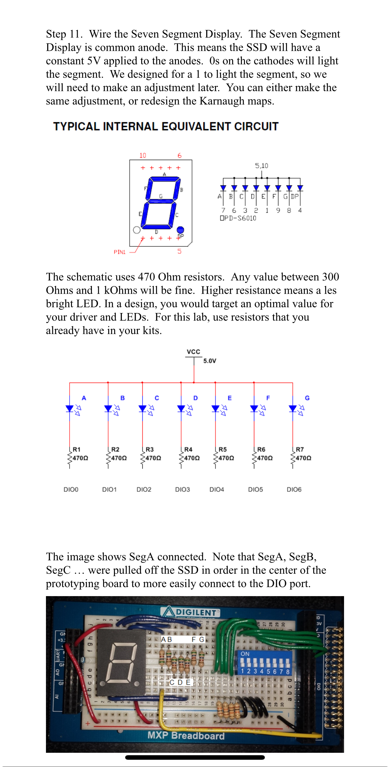
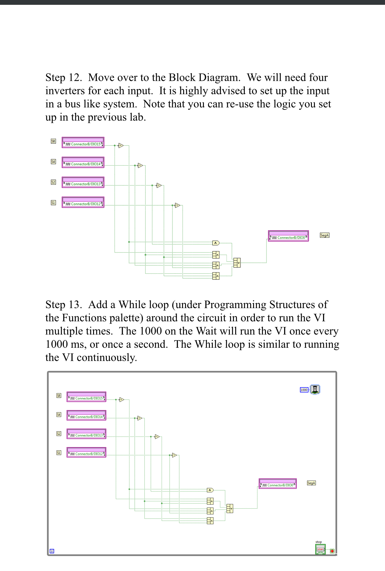
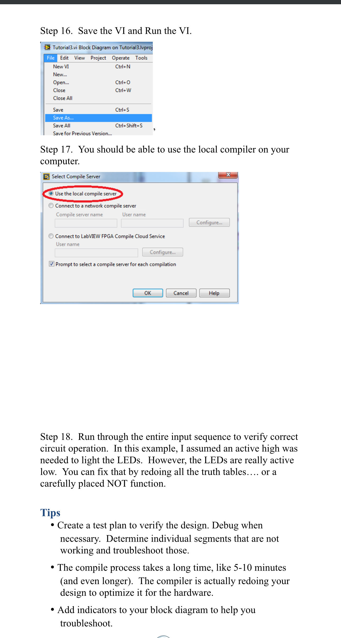
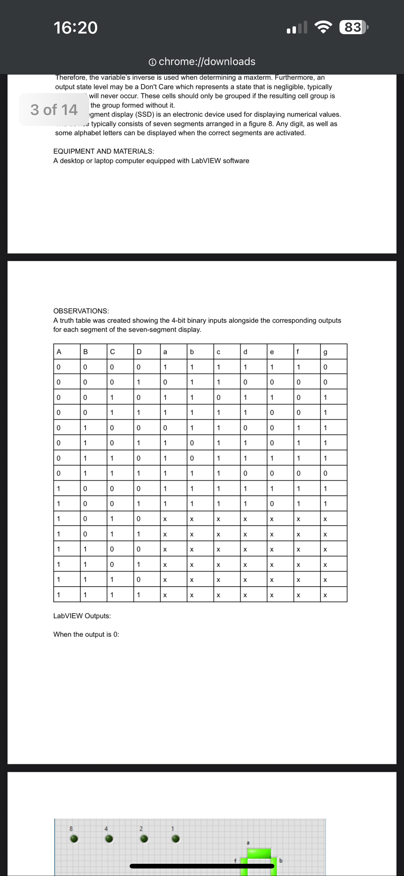
Lab 3 Karnaugh Maps Due Date: Sunday of Week 6 by 11:55 PM In this lab experiment, the student will implement a minimized, seven-segment display decoder circuit using Karnaugh maps. This lab requires knowledge of Karnaugh map simplification which is briefly discussed in the Background & Theory section of this lab handout. [z Objectives Y Create minimal logic circuits using Karnaugh map simplification. /Y Design a minimal seven-segment display decoder. Y Download the circuit to LabVIEW @ Pre-Lab Preparation pe For this lab, you will design digital hardware to interface with a seven-segment display module. Read the following manual and note the layout of the segments as well as their assigned pins: Use the Boolean equations you designed and simulated in lab 2 and implement the circuit on the FPGA in the myRIO. x+y=3 Background & Theory Seven Segment Display A seven-segment display (SSD) is an electronic device used for displaying numerical values. The device typically consists of seven segments arranged in a figure 8. Any digit, as well as some alphabet letters, can be displayed when the correct segments are activated. An example of an SSD as well as possible outputs can be seen in Figure 3. Figure 1 - Seven-Segment Display with Numeric Outputs Workstation Details PC Desktop / Laptop with Lab VIEW FPGA 2013 NI ELVIS II NI myRIO with components Lab Procedure Task Using the Boolean equations created in Lab 2, implement minimal logic circuits in Lab VIEW FPGA for each segment output of the SSD using myRIO. Requirements . Use slide switches as inputs, as shown below . Connect outputs to the appropriate I/O port pins connected to the seven-segment display module for segment 0. . Create a test plan to verify the design. Debug when necessary. . Take pictures showing all numbers 0 through 9 on your FPGA topboard.Step 1. Open Lab VIEW on your computer LabVIEW 2015 (32-bit) LabVIEW 2015 (32-bit) Help LabVIEW 2015 (32-bit) Manuals LabVIEW 2015 (32-bit) Readme LabVIEW 2015 (32-bit) NI ELVISmx for NI ELVIS & NI myDA NI FlexRIO NI-DAQ NI-DAQmx NI-Serial NI-VISA R Series Multifunction RIO Real-Time Trace Viewer 2015 Back Search programs and files e D Step 2. Create a new Project LabVIEW OX File Operate Tools Help LabVIEW myRIO 2015 Search Q Create Project Open Existing Recent Project Templates AllStep 3. Select myRIO Custom FPGA Project under the myRIO template. Create Project Choose a starting point for the project: All Blank Project Templates Templates Creates a blank project. Desktop myRIO Sample Projects myRIO Project Templates CompactRIO Creates a new project for controlling your myRIO. This template uses code written with the Desktop LabVIEW myRIO Toolkit. More Information myRIO myRIO Custom FPGA Project Templates Real-Time Facilitates customizing the myRIO FPGA personality. This template uses code written with the abVIEW FPGA Module. More Information Step 4. Create a Project name and define the path. This myRIO is connected through WiFi. If your myRIO is plugged in, select the appropriate option. Click Finish once complete. Create Project Configure the new project: myRIO Custom FPGA Project Project Name Lab3 Project Root C: \\Lab3 File Name Prefix (Optional) Target Plugged into USB NI-myRIO-1900-03058172 (192.168.2.16) Connected over WiFi Generic Target Specific IP Address or Hostname FPGA Personality Default Supports general 1/O, protocols, and interrupt. Learn more mu SPI UART - !IRQ DIO Button LED 2 ACC PWM ENC 12C UART IRQ Back Finish Cancel HelpStep 5. In the Project Explorer window, right-click FPGA Target, and select New -> VI De Lab3.lvproj - Project Explorer X File Edit View Project Operate Tools Window Help Items Files . : Project: Lab3.lvproj My Computer Project Documentation Build Specifications NI-myRIO-1900-03058172 (192.168.2.16) -. $53 Chassis (myRIO-1900) FPGA Target (RIO0, myRIO- New VI Audio Virtual Folder ConnectorA Select Execution Mode ConnectorB Control ConnectorC RIO Device Setup... Library Onboard 1/O Add Class $4800000 Sub VIs 40 MHz Onboard Clock Find Project Items... FPGA 1/O FPGA Main Default.vi FPGA Base Clock Arrange By Ill A.DO1 DMA HIP A.DIO DMA Expand All Register Handshake HIk A.AIO DMA Collapse All Memory HIk A.AOO DMA Remove from Project FIFO Ill AudioIn DMA Rename... F2 Component-Level IP Ill AudioOut DMA +. ] IP Builder Help... Build Specifications Properties RT Main.vi Build SpecificationsStep 6. For this demonstration, we will implement Segment A Inputs SegA S8S4S2S1 Z 0000 1 0001 0 Note that a tail was placed on the 6. That is optional for you in the lab. You can also make the outputs for 10-15 as don't cares, if you wish. The Boolean equation for this truth table is SegA = S8'*S2 + S8*S4?*S82' + S8*S4*S1 + S4'*S82*S1' Step 7. First, we will configure the inputs. Drag the ConnectorB/DIO15 to ConnectorB/DIO12 from the Project Explorer to the Block Diagram. Lab3.lvproj * - Project Explorer -O X File Edit View Project Operate Tools Window Help Items Files . Project: Lab3.lvproj . My Computer Project Documentation Build Specifications NI-myRIO-1900-03058172 (192.168.2.16) 3. 453 Chassis (myRIO-1900 FPGA Target (RIO0, myRIO-1900) +. Audio "MW ConnectorB/DIO15 ConnectorA ConnectorB Analog DIO7:0 "M ConnectorB/DIO14 DIO15:8 + ConnectorB/DIO8 + ConnectorB/D109 + ConnectorB/DIO10 JU ConnectorB/DIO13 9 + ConnectorB/DIO11 ConnectorB/DIO12 + ConnectorB/DIO13 a+ ConnectorB/DIO14 JUU ConnectorB/DIO124 ConnectorB/DIO15 + ConnectorB/DIO15:8 ConnectorC Onboard 1/O Sub VIs #9 40 MHz Onboard Clock FPGA Main Default.vi HIP A.DO1 DMA HIP A.DIO DMA HIP A.AIO DMAWire the switch inputs to Port B of the myRIO. You can use any switches that you want, but be sure to put the most significant switch (worth 8) on the left. In the image below, the switch marked 1 is worth 8, the switch marked 2 is worth 4, the switch marked 3 is worth 2, and the switch marked 4 is worth 1. The schematic and image are shown below. Note that a 0 is generated when the switch is flipped up and a 1 is generated when the switch is down. There are other possible ways to connect the switches. VCC 5.0V R4 R1 R2 R3 10kQ 10kQ 10kQ 10kQ DIO15 DIO14 DIO13 DIO12 S2 S1 IS8 S4 A DIGILENT - u u ON 2 AO QUART 12 3 cd abcde MXP Breadboard Step 8. Place the segment outputs on the Block Diagram from the Project Explorer.. [ Lab3./vproj * - Project Explorer File Edit View Project Operate Tools Window Help Fu ConnectorB/DICO; Items Files Project: Lab3.Ivproj nu ConnectorB/ Project Docume Build Specifications . Ni-myRIO-1900-03058172 (192.168.216) as Chassis (myRIO-1900) OFPGA Taro Target (8100, myRIO-1900) Audio TV ConnectorBVDIO15 ConnectorA ConnectorB An TV Connector8/010139 I ConnectorB/01012 N Connectorevolost " Al Connector8/6105Step 9. Configure the segment outputs to outputs by right clicking the border and selecting Change to Write. Note that you need to click in the exact right spot to get the Change to Write option to appear. So keep trying if you do not see it at first. == a tne Pa : Visible Items > Help Description and Tip... Breakpoint > FPGA I/O Palette Boolean Palette Create Replace Find FPGA I/O in Project Show Error Terminals CGF Tale om ini Add Element Add New FPGA I/O... Select FPGA I/O Properties Remove and Rewire Sy Siu ConnectorB/DIO6 9] Step 10. It is highly recommended to add text to your VI to label the inputs and output accordingly. This just makes it easier for you to insure you are selecting the correct input/output. ie eo Bl FY 5 & 3 | E Gi | 3 3 S | a Note that these steps are only going to focus on SegA. So other segments will not be shown for the remainder of this lab. Step 11. Wire the Seven Segment Display. The Seven Segment Display is common anode. This means the SSD will have a constant 5 V applied to the anodes. Os on the cathodes will light the segment. We designed for a 1 to light the segment, so we will need to make an adjustment later. You can either make the same adjustment, or redesign the Karnaugh maps. TYPICAL INTERNAL EQUIVALENT CIRCUIT 10 + + + + + 5,10 G ABCDEFG DP 6 3 2 9 8 OPD-S6010 + + + PINI The schematic uses 470 Ohm resistors. Any value between 300 Ohms and 1 kOhms will be fine. Higher resistance means a les bright LED. In a design, you would target an optimal value for your driver and LEDs. For this lab, use resistors that you already have in your kits. VCC 5.0V A E C D F G 4 4 4 R1 R2 R3 R4 R5 R6 R7 24700 24700 24700 24700 24700 24700 $4700 DIOO DIO1 DIO2 DIO3 DIO4 DIO5 DIO6 The image shows SegA connected. Note that SegA, SegB, SegC ... were pulled off the SSD in order in the center of the prototyping board to more easily connect to the DIO port. A DIGILENT - NM AB F G ON UART GF AO 5 6 7 abcde CDE + MXP BreadboardStep 12. Move over to the Block Diagram. We will need four inverters for each input. It is highly advised to set up the input in a bus like system. Note that you can re-use the logic you set up in the previous lab. (i BAS & EY Step 13. Adda While loop (under Programming Structures of the Functions palette) around the circuit in order to run the VI multiple times. The 1000 on the Wait will run the VI once every 1000 ms, or once a second. The While loop is similar to running the VI continuously. TW ConnectorB/DI0125 Step 16. Save the VI and Run the VI. . 4 Tutorial3.vi Block Diagram on Tutorial3.lvproj Edit View Project Operate Tools New VI Ctrl+N New... Open... Ctri+O Close Ctrl+W Close All Save Ctrl+S Save All Ctrl+Shift+S Save for Previous Version... Step 17. You should be able to use the local compiler on your computer. {G3 Select Compile Server a i x '@) Use the local compile server ) Connect to a network compile server Compile server name User name Configure... ~) Connect to LabVIEW FPGA Compile Cloud Service } User name Configure. | Prompt to select a compile server for each compilation Step 18. Run through the entire input sequence to verify correct circuit operation. In this example, I assumed an active high was needed to light the LEDs. However, the LEDs are really active low. You can fix that by redoing all the truth tables.... or a carefully placed NOT function. Tips * Create a test plan to verify the design. Debug when necessary. Determine individual segments that are not working and troubleshoot those. * The compile process takes a long time, like 5-10 minutes (and even longer). The compiler is actually redoing your design to optimize it for the hardware. * Add indicators to your block diagram to help you troubleshoot. Conclusion Questions * Describe in detail the test plan used to verify the design, as well as the debugging process used to correct any errors. * How does simulation, like in Lab 2, help in the design process? Lab Report Submit an individual lab report by Sunday of Week 6 at 11:55 PM following the standard lab report template @ chrome://downloads erefore, the variable's inverse is used when determining a maxterm. Furthermore, an output state level may be a Don't Care which represents a state that is negligible, typically * will never occur. These cells should only be grouped if the resulting cell group is 3 of 1 4 the group formed without it. :gment display (SSD) is an electronic device used for displaying numerical values. - typically consists of seven segments arranged in a figure 8, Any digit, as well as some alphabet letters can be displayed when the correct segments are activated. EQUIPMENT AND MATERIALS: A desktop or laptop computer equipped with LabVIEW software OBSERVATIONS: A truth table was created showing the 4-bit binary inputs alongside the corresponding outputs for each segment of the seven-segment display. LabVIEW Outputs: When the output is 0
Step by Step Solution
There are 3 Steps involved in it
1 Expert Approved Answer
Step: 1 Unlock
Question Has Been Solved by an Expert!
Get step-by-step solutions from verified subject matter experts
Step: 2 Unlock
Step: 3 Unlock
Students Have Also Explored These Related Accounting Questions!