

Question: please step by step and clear QI (a) A PLD is a general-purpose chip for implementing logic circuits. It contains a collection of logic circuit
please step by step and clear
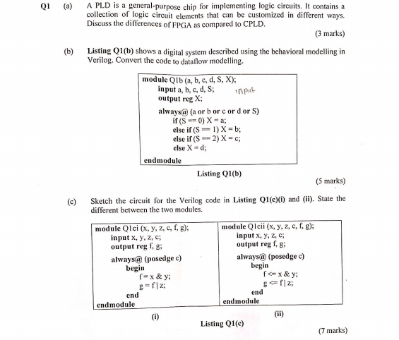
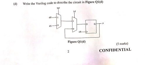
QI (a) A PLD is a general-purpose chip for implementing logic circuits. It contains a collection of logic circuit elements that can be customized in different ways. Discuss the differences of FPGA as compared to CPLD. (3 marks) (6) Listing Q1(b) shows a digital system described using the behavioral modelling in Verilog. Convert the code to dataflow modelling. module Q1b (a, b, c, d, S, X); input a, b, c, d, S: input output reg X; always@ (a or b or cord or S) if(s ==0) X - a; else if(s == 1)X = b; else if ( S2) X=c; else X -d; endmodule Listing Q1(b) (5 marks) (c) Sketch the circuit for the Verilog code in Listing Q1(c)) and (ii). State the different between the two modules. module Qlci (x, y, z, c, , g): module Qlcii (x, y, 2, C, fig); input x, y, z, input x, y, z, ; output regfg output reg f.g always@ (posedge c) always@ (posedge c) begin begin fax&y; fox & y g=f|z; gwf|z; end end endmodule endmodule (0) Listing Q10 (7 marks) (d) Write the Verilog code to describe the circuit in Figure Q1(d) Sel ud db D di 0 o Figure Q1(d) (5 marks) CONFIDENTIAL 2 QI (a) A PLD is a general-purpose chip for implementing logic circuits. It contains a collection of logic circuit elements that can be customized in different ways. Discuss the differences of FPGA as compared to CPLD. (3 marks) (6) Listing Q1(b) shows a digital system described using the behavioral modelling in Verilog. Convert the code to dataflow modelling. module Q1b (a, b, c, d, S, X); input a, b, c, d, S: input output reg X; always@ (a or b or cord or S) if(s ==0) X - a; else if(s == 1)X = b; else if ( S2) X=c; else X -d; endmodule Listing Q1(b) (5 marks) (c) Sketch the circuit for the Verilog code in Listing Q1(c)) and (ii). State the different between the two modules. module Qlci (x, y, z, c, , g): module Qlcii (x, y, 2, C, fig); input x, y, z, input x, y, z, ; output regfg output reg f.g always@ (posedge c) always@ (posedge c) begin begin fax&y; fox & y g=f|z; gwf|z; end end endmodule endmodule (0) Listing Q10 (7 marks) (d) Write the Verilog code to describe the circuit in Figure Q1(d) Sel ud db D di 0 o Figure Q1(d) (5 marks) CONFIDENTIAL 2
Step by Step Solution
There are 3 Steps involved in it

Get step-by-step solutions from verified subject matter experts