

Question: PLEASE WRITE A VERILOG MODULE myALU4 IN PROBLEM 4. thank you I. OBJECTIVES In this laboratory you will: Design and test a 4-bit arithmetic logic
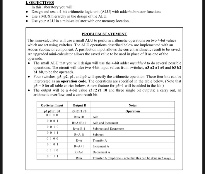
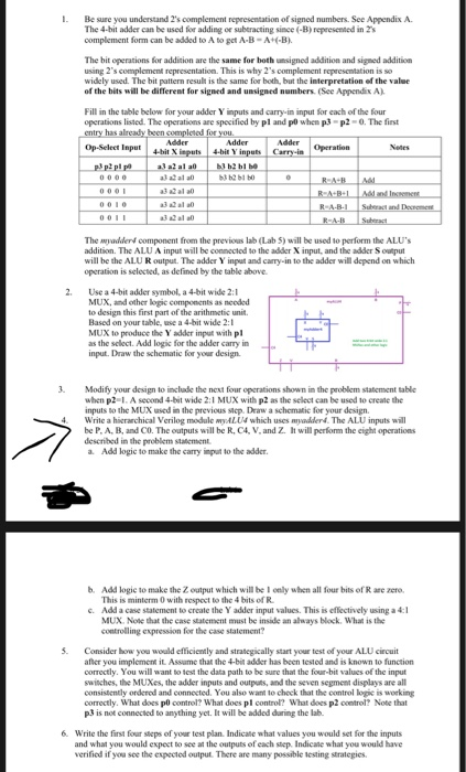
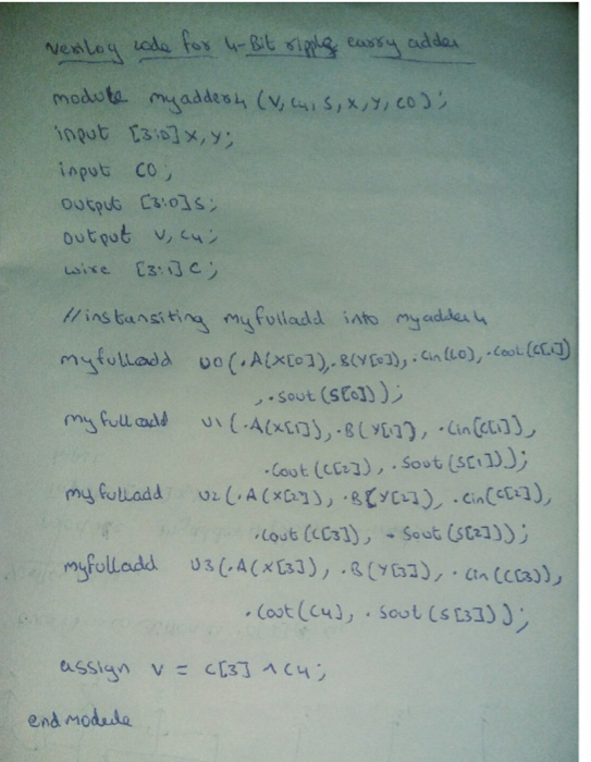
I. OBJECTIVES In this laboratory you will: Design and test a 4-bit arithmetic logic unit (ALU) with adder/subtractor functions Use a MUX hierarchy in the design of the ALU. Use your ALU in a mini-calculator with one memory location. PROBLEM STATEMENT The mini-calculator will use a small ALU to perform arithmetic operations on two 4-bit values which are set using switches. The ALU operations described below are implemented with an Adder/Subtractor component. A pushbutton input allows the current arithmetic result to be saved An upgraded mini-calculator allows the saved value to be used in place of B as one of the operands. The small ALU that you will design will use the 4-bit adder myadder to do several possible operations. The circuit will take two 4-bit input values from switches, a3 a2 al a0 and b3 b2 b1 b0, to be the operands. Four switches, p3, p2, p1, and po will specify the arithmetic operation. These four bits can be interpreted as an operation code. The operations are specified in the table below. (Note that p3 = 0 for all table entries below. A new feature for p3=1 will be added in the lab.) The output will be a 4-bit value r3 r2 r1 r0 and three single bit outputs: a carry out, an arithmetic overflow, and a zero result bit. Op-Select Input p3 p2 pl po 0 000 Output R r3 r2 r1 ro R A+B Notes Operation Add 0001 | R A+B+| R A-B-1 Add and Increment Subtract and Decrement Subtract | RUA-B 0010 0011 0100 0101 0110 0111 Transfer A Increment A REA R-A+1 R-A-1 - RA Decrement A Transfer A (duplicate - note that this can be done in 2 ways. Be sure you understand 2's complement representation of signed numbers. See Appendix A The 4-bit adder can be used for adding or eracting since (-) presented in s complement form can be added to A to get A-B-A -B The bit operations for addition are the same for both unsigned addition and signed addition using 2's complement representation. This is why 2's complement representation is so widely used. The hit p er result is the same for both but the interpretation of the value of the hits will be different for signed and unsigned aubers(See Appendix A) Wider Fill in the table below for your adder Yinputs and carry input for each of the four operations listed. The operations are specified by pl w hen p -p2-. The first try has already been completed for you Adder Adder 4- pits Yeu Ca p rice ppp al at RAM DI The added component from the previous ab Labs) will be used to perform the ALU' addition. The ALU A input will be connected to the addier X input, and the adder Soutput will be the ALU R output. The adder Yinput and carryin to the adder will depend on which operation is selected, as defined by the table above Use a 4-bit adder symbol, a 4-bit wide 2:1 MUX, and other logic components as needed to design this first part of the arithmetic unit Based on your while we a 4-bit wide 2:1 MUX to produce the Yadder input with pl as the select. Add logic for the adder carry in input. Draw the schematic for your design Modify your design to include the next four operations shown in the problem statement le when p2-1. A Second 4.but wide 2:1 MUX with p2 as the select can be used to create the inputs to the MUX used in the previous stop. Draw a schematic for your design Write a hierarchical Verilog module ALU which uses w e rd The ALU inputs will be P.A.B and CO. The outputs will be R. C4, V. and Z. It will perform the ciht operations described in the problem statement Add logic to make the carry input to the adder Add logic to make the output which will be cely when all for its of Rwe This is minder with respect to the 4 hits of R Add a case statical create the Yder v al This cflct MUX. Note that the case samen met be made analys Block. What is the collage for the casetament 41 Consider how you would efficiently and strategically start your best of your ALU for you implement Ass that the header has been tested and is known to function Correctly. You will want to test the data path to be sure that the four-hit values of the input wiches, the MUXes, the addermus and outputs and the seven segment displays are all Cos tly dened and woted. You are we to check that the control is working Correctly. What doespool What does plc What does p or Not that p3 is not connected to anything yet. It will be added during the la 6. While the first four steps of your best plan. Indicate that values you would set for the inputs and what you would expect to the outputs of each step. Indicate what you would have verified if you see the expected output. There are many possible testing strategies Neslog code for 4-Bit ripple cassy adder module my addess (V, 4, 5, x, y, co ) input [30]x,y; input co output [3:0]; output u, cu wire [3:13c; Hinstansiting my fulladd into my addest myfulladd o (Alx[01), 807[]), in (LO),.coot () .sout (S[o])); my full cadd vi(-A(X[1]), B(Y[1]), (in (c[1]], Cout (C[2]), Sout (s[1])); my fulladd v2 (.A (X[2]), B8y (23) . Cin (C[2]), Lout (C[3]) - Sout (5[2])); myfulladd U3(-A(X[3]), B(Y [3]), (in (C13)), Cout (cul, sout (5[3])) ; assign vec[3] 164; end modele I. OBJECTIVES In this laboratory you will: Design and test a 4-bit arithmetic logic unit (ALU) with adder/subtractor functions Use a MUX hierarchy in the design of the ALU. Use your ALU in a mini-calculator with one memory location. PROBLEM STATEMENT The mini-calculator will use a small ALU to perform arithmetic operations on two 4-bit values which are set using switches. The ALU operations described below are implemented with an Adder/Subtractor component. A pushbutton input allows the current arithmetic result to be saved An upgraded mini-calculator allows the saved value to be used in place of B as one of the operands. The small ALU that you will design will use the 4-bit adder myadder to do several possible operations. The circuit will take two 4-bit input values from switches, a3 a2 al a0 and b3 b2 b1 b0, to be the operands. Four switches, p3, p2, p1, and po will specify the arithmetic operation. These four bits can be interpreted as an operation code. The operations are specified in the table below. (Note that p3 = 0 for all table entries below. A new feature for p3=1 will be added in the lab.) The output will be a 4-bit value r3 r2 r1 r0 and three single bit outputs: a carry out, an arithmetic overflow, and a zero result bit. Op-Select Input p3 p2 pl po 0 000 Output R r3 r2 r1 ro R A+B Notes Operation Add 0001 | R A+B+| R A-B-1 Add and Increment Subtract and Decrement Subtract | RUA-B 0010 0011 0100 0101 0110 0111 Transfer A Increment A REA R-A+1 R-A-1 - RA Decrement A Transfer A (duplicate - note that this can be done in 2 ways. Be sure you understand 2's complement representation of signed numbers. See Appendix A The 4-bit adder can be used for adding or eracting since (-) presented in s complement form can be added to A to get A-B-A -B The bit operations for addition are the same for both unsigned addition and signed addition using 2's complement representation. This is why 2's complement representation is so widely used. The hit p er result is the same for both but the interpretation of the value of the hits will be different for signed and unsigned aubers(See Appendix A) Wider Fill in the table below for your adder Yinputs and carry input for each of the four operations listed. The operations are specified by pl w hen p -p2-. The first try has already been completed for you Adder Adder 4- pits Yeu Ca p rice ppp al at RAM DI The added component from the previous ab Labs) will be used to perform the ALU' addition. The ALU A input will be connected to the addier X input, and the adder Soutput will be the ALU R output. The adder Yinput and carryin to the adder will depend on which operation is selected, as defined by the table above Use a 4-bit adder symbol, a 4-bit wide 2:1 MUX, and other logic components as needed to design this first part of the arithmetic unit Based on your while we a 4-bit wide 2:1 MUX to produce the Yadder input with pl as the select. Add logic for the adder carry in input. Draw the schematic for your design Modify your design to include the next four operations shown in the problem statement le when p2-1. A Second 4.but wide 2:1 MUX with p2 as the select can be used to create the inputs to the MUX used in the previous stop. Draw a schematic for your design Write a hierarchical Verilog module ALU which uses w e rd The ALU inputs will be P.A.B and CO. The outputs will be R. C4, V. and Z. It will perform the ciht operations described in the problem statement Add logic to make the carry input to the adder Add logic to make the output which will be cely when all for its of Rwe This is minder with respect to the 4 hits of R Add a case statical create the Yder v al This cflct MUX. Note that the case samen met be made analys Block. What is the collage for the casetament 41 Consider how you would efficiently and strategically start your best of your ALU for you implement Ass that the header has been tested and is known to function Correctly. You will want to test the data path to be sure that the four-hit values of the input wiches, the MUXes, the addermus and outputs and the seven segment displays are all Cos tly dened and woted. You are we to check that the control is working Correctly. What doespool What does plc What does p or Not that p3 is not connected to anything yet. It will be added during the la 6. While the first four steps of your best plan. Indicate that values you would set for the inputs and what you would expect to the outputs of each step. Indicate what you would have verified if you see the expected output. There are many possible testing strategies Neslog code for 4-Bit ripple cassy adder module my addess (V, 4, 5, x, y, co ) input [30]x,y; input co output [3:0]; output u, cu wire [3:13c; Hinstansiting my fulladd into my addest myfulladd o (Alx[01), 807[]), in (LO),.coot () .sout (S[o])); my full cadd vi(-A(X[1]), B(Y[1]), (in (c[1]], Cout (C[2]), Sout (s[1])); my fulladd v2 (.A (X[2]), B8y (23) . Cin (C[2]), Lout (C[3]) - Sout (5[2])); myfulladd U3(-A(X[3]), B(Y [3]), (in (C13)), Cout (cul, sout (5[3])) ; assign vec[3] 164; end modele
Step by Step Solution
There are 3 Steps involved in it

Get step-by-step solutions from verified subject matter experts