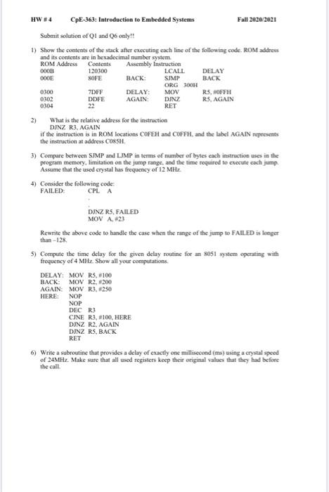
Question: plese solve only 1&6 HW#4 CpE-363: Introduction to Embedded Systems Fall 2020/2021 Submit solution of QI and Q6 only!! 1) Show the contents of the

HW#4 CpE-363: Introduction to Embedded Systems Fall 2020/2021 Submit solution of QI and Q6 only!! 1) Show the contents of the stack after executing cach line of the following code ROM address and its contents are in hexadecimal number system ROM Address Contents Assembly Instruction 120300 LCALL DELAY 000E 80FE BACK: SJMP BACK ORG 300H 0300 7DFF DELAY: MOV RS, OFFH 0302 DDFE AGAIN: DJNZ RS. AGAIN 0304 22 RET 2) What is the relative address for the instruction DINZ R3. AGAIN if the instruction is in ROM locations COFEH and COFFH, and the label AGAIN represents the instruction at address COSSH 3) Compare between SJMP and LIMP in terms of number of bytes each instruction uses in the program memory, limitation on the jump rangea the required to execute cach jump Assume that the used crystal has frequency of 12 MHz 4) Consider the following code FAILED CPLA DJNZ R5, FAILED MOV A. #23 Rewrite the above code to handle the case when the range of the jump to FAILED is longer than-128 5) Compute the time delay for the given delay routine for an 8051 system operating with frequency of 4 MHz Show all your computations DELAY: MOV RS, #100 BACK MOV R2,200 AGAIN: MOV R3, #250 HERE NOP NOP DEC R3 CUNE R3, #100, HERE DJNZ R2, AGAIN DINZ RS, BACK RET 6) Write a subroutine that provides a delay of exactly one millisecond (ms) using a crystal speed of 24MHz. Make sure that all used registers keep their original values that they had before the call
Step by Step Solution
There are 3 Steps involved in it

Get step-by-step solutions from verified subject matter experts


