

Question: Problem 2 : p - i - n Diode A p - i - n diode is a semiconductor diode with a wide, lightly doped
Problem : pin Diode
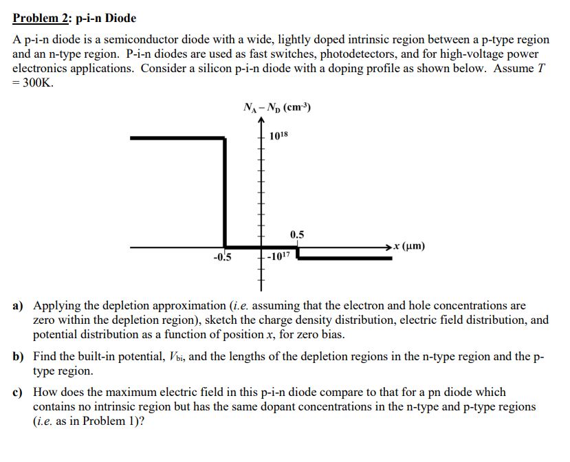
A pin diode is a semiconductor diode with a wide, lightly doped intrinsic region between a ptype region and an ntype region. Pin diodes are used as fast switches, photodetectors, and for highvoltage power electronics applications. Consider a silicon pin diode with a doping profile as shown below. Assume T mathrm~K
a Applying the depletion approximation ie assuming that the electron and hole concentrations are zero within the depletion region sketch the charge density distribution, electric field distribution, and potential distribution as a function of position x for zero bias.
b Find the builtin potential, Vmathrmbi and the lengths of the depletion regions in the ntype region and the ptype region.
c How does the maximum electric field in this pin diode compare to that for a pn diode which contains no intrinsic region but has the same dopant concentrations in the ntype and ptype regions ie as in Problem
Step by Step Solution
There are 3 Steps involved in it
1 Expert Approved Answer
Step: 1 Unlock

Question Has Been Solved by an Expert!
Get step-by-step solutions from verified subject matter experts
Step: 2 Unlock
Step: 3 Unlock