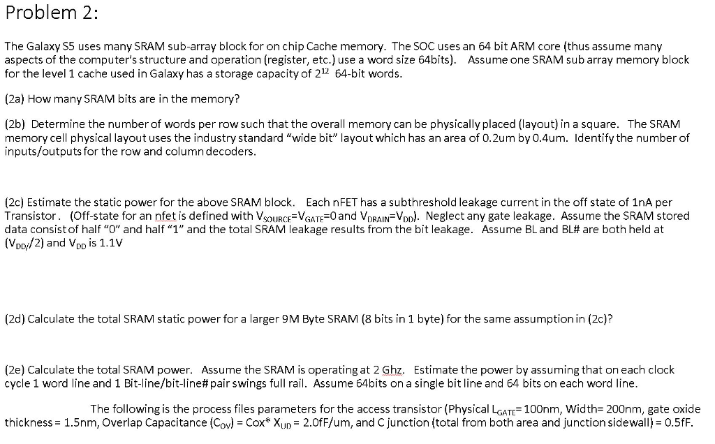
Question: Problem 2: The Galaxy S5 uses many SRAM sub-array block for on chip Cache memory. The SOC uses an 64 bit ARM core (thus assume

Problem 2: The Galaxy S5 uses many SRAM sub-array block for on chip Cache memory. The SOC uses an 64 bit ARM core (thus assume many aspects of the computer's structure and operation (register, etc.) use a word size 64bits). Assume one SRAM sub array memory block for the level 1 cache used in Galaxy has a storage capacity of 212 64-bit words. (2a) How many SRAM bits are in the memory? (2b) Determine the number of words per row such that the overall memory can be physically placed (layout) in a square. The SRAM memory cell physical layout uses the industry standard "wide bit" layout which has an area of 0.2um by 0.4um. Identify the number of inputs/outputs for the row and column decoders (2c) Estimate the static power for the above SRAM block. Each nFET has a subthreshold leakage current in the off state of 1nA per Transistor. (Off-state for an nfet is defined with VsOURCE VGATE 0and VDRAIN V). Neglect any gate leakage. Assume the SRAM storec data consist of half"0" and half "1" and the total SRAM leakage results from the bit leakage. Assume BL and BL# are both held at (VDo//2) and Voo is 1.1V (2d) Calculate the total SRAM static power for a larger 9M Byte SRAM (8 bits in 1 byte) for the same assumption in (2c)? (2e) Calculate the total SRAM power. Assume the SRAM is operating at 2 Ghz. Estimate the power by assuming that on each clock Cycle 1 word line and 1 Bit-line/bit-line#pair swings full rail. Assume 64bits on a single bit line and 64 bits on each word line. The following is the process files parameters for the access transistor (Physical LGATE 100nm, Width- 200nm, gate oxide thickness = 1.5 nm Overlap Capacitance Co-Cox"XUD-2.0fF/um, and C junction total from both area and unction sidew all-0.5 Problem 2: The Galaxy S5 uses many SRAM sub-array block for on chip Cache memory. The SOC uses an 64 bit ARM core (thus assume many aspects of the computer's structure and operation (register, etc.) use a word size 64bits). Assume one SRAM sub array memory block for the level 1 cache used in Galaxy has a storage capacity of 212 64-bit words. (2a) How many SRAM bits are in the memory? (2b) Determine the number of words per row such that the overall memory can be physically placed (layout) in a square. The SRAM memory cell physical layout uses the industry standard "wide bit" layout which has an area of 0.2um by 0.4um. Identify the number of inputs/outputs for the row and column decoders (2c) Estimate the static power for the above SRAM block. Each nFET has a subthreshold leakage current in the off state of 1nA per Transistor. (Off-state for an nfet is defined with VsOURCE VGATE 0and VDRAIN V). Neglect any gate leakage. Assume the SRAM storec data consist of half"0" and half "1" and the total SRAM leakage results from the bit leakage. Assume BL and BL# are both held at (VDo//2) and Voo is 1.1V (2d) Calculate the total SRAM static power for a larger 9M Byte SRAM (8 bits in 1 byte) for the same assumption in (2c)? (2e) Calculate the total SRAM power. Assume the SRAM is operating at 2 Ghz. Estimate the power by assuming that on each clock Cycle 1 word line and 1 Bit-line/bit-line#pair swings full rail. Assume 64bits on a single bit line and 64 bits on each word line. The following is the process files parameters for the access transistor (Physical LGATE 100nm, Width- 200nm, gate oxide thickness = 1.5 nm Overlap Capacitance Co-Cox"XUD-2.0fF/um, and C junction total from both area and unction sidew all-0.5
Step by Step Solution
There are 3 Steps involved in it

Get step-by-step solutions from verified subject matter experts


