

Question: Problem 3 ( 2 0 points ) A P - N junction is created by doping the left side of a piece of silicon with
Problem points
A PN junction is created by doping the left side of a piece of silicon with atoms of phosphorus and the right side with atomscm of boron. Assume that the dopants are fully ionized, and assume the junction is at with pointed to the right. Assume that the band gap of silicon is and that and do not change with temperature.
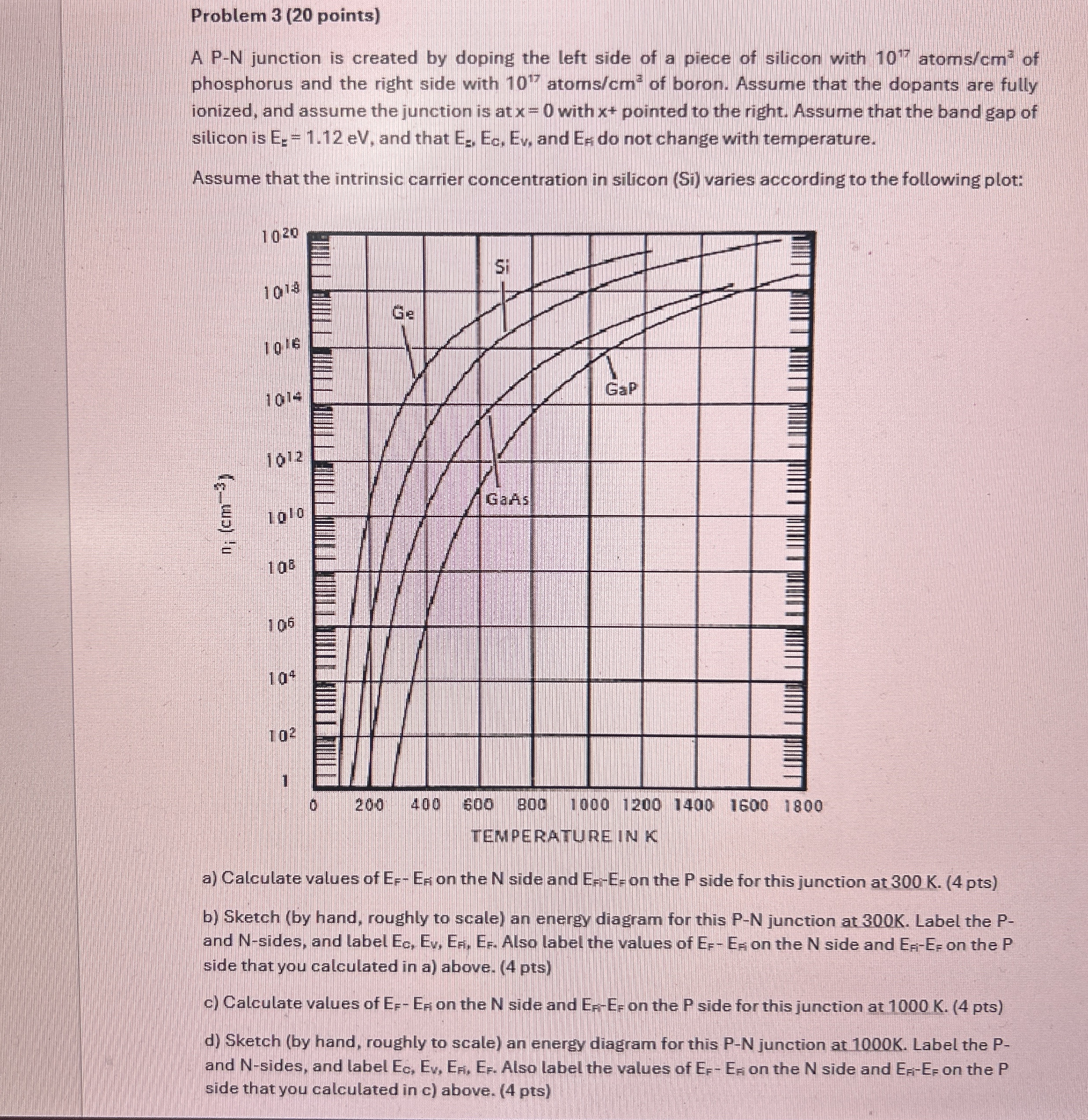
Assume that the intrinsic carrier concentration in silicon Si varies according to the following plot:
TEMPERATUREINK
a Calculate values of on the side and the side for this junction at K pts
b Sketch by hand, roughly to scale an energy diagram for this PN junction at K Label the P and sides, and label Also label the values of on the side and on the side that you calculated in a above. pts
c Calculate values of on the side and on the side for this junction at K pts
d Sketch by hand, roughly to scale an energy diagram for this PN junction at K Label the Pand sides, and label Also label the values of on the side and on the side that you calculated in c above. pts
Step by Step Solution
There are 3 Steps involved in it
1 Expert Approved Answer
Step: 1 Unlock

Question Has Been Solved by an Expert!
Get step-by-step solutions from verified subject matter experts
Step: 2 Unlock
Step: 3 Unlock