

Question: Problem 3 : Common - Emitter Voltage Amplifier Analysis ( 0 to 3 5 points ) Figure 3 : Common Emitter Amplifier This PSPICE activity
Problem : CommonEmitter Voltage Amplifier Analysis to points
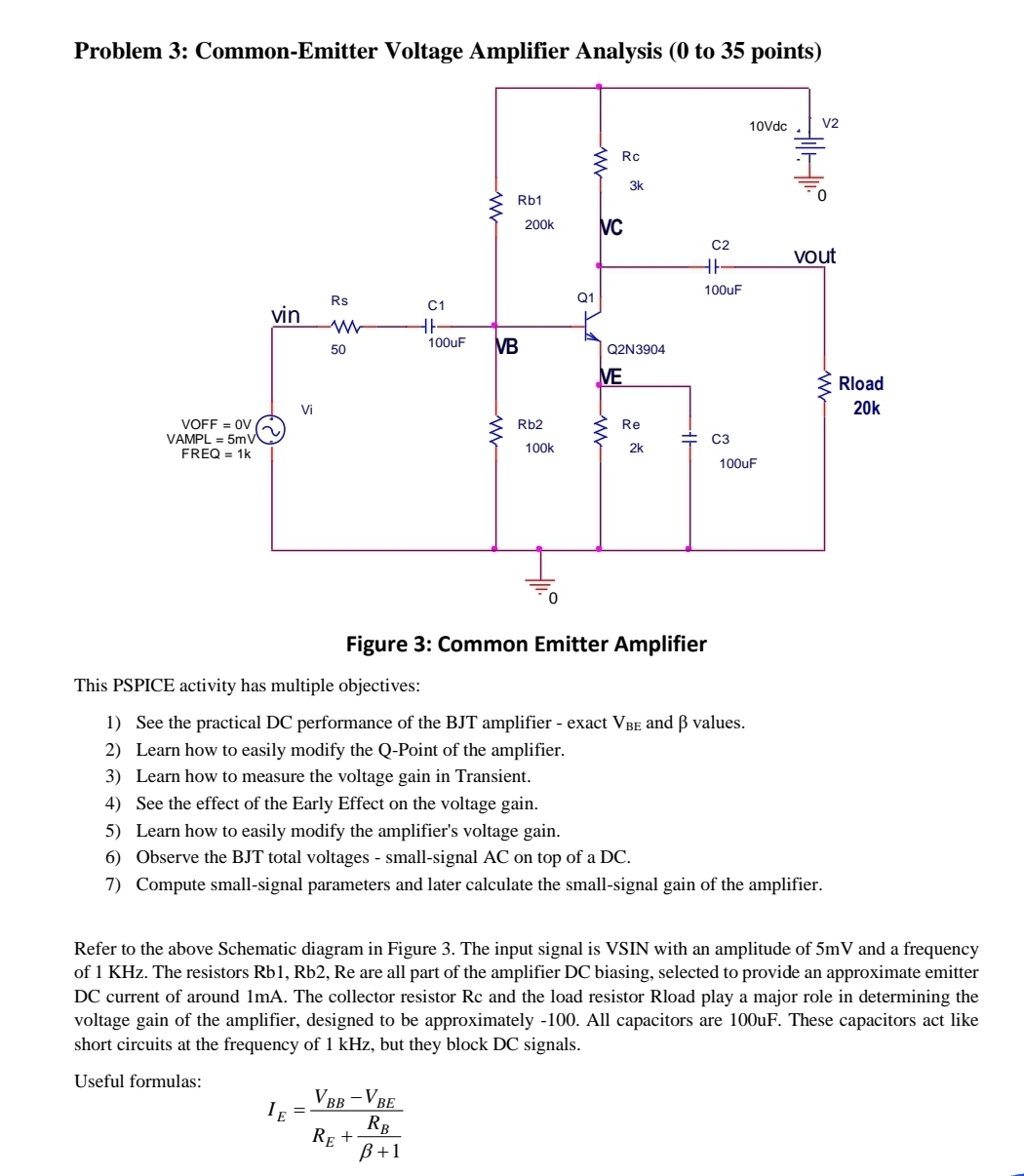
Figure : Common Emitter Amplifier
This PSPICE activity has multiple objectives:
See the practical DC performance of the BJT amplifier exact and values.
Learn how to easily modify the QPoint of the amplifier.
Learn how to measure the voltage gain in Transient.
See the effect of the Early Effect on the voltage gain.
Learn how to easily modify the amplifier's voltage gain.
Observe the BJT total voltages smallsignal AC on top of a DC
Compute smallsignal parameters and later calculate the smallsignal gain of the amplifier.
Refer to the above Schematic diagram in Figure The input signal is VSIN with an amplitude of mV and a frequency of KHz The resistors are all part of the amplifier DC biasing, selected to provide an approximate emitter DC current of around mA The collector resistor Rc and the load resistor Rload play a major role in determining the voltage gain of the amplifier, designed to be approximately All capacitors are uF These capacitors act like short circuits at the frequency of kHz but they block DC signals.
Useful formulas:
Step by Step Solution
There are 3 Steps involved in it
1 Expert Approved Answer
Step: 1 Unlock

Question Has Been Solved by an Expert!
Get step-by-step solutions from verified subject matter experts
Step: 2 Unlock
Step: 3 Unlock