

Question: Problem 3: Sizing for Performance and Energy Assume the inverters are implemented in standard CMOS and have symmetrical VTC. Assume Cintrinsic = Cgate (r= 1).
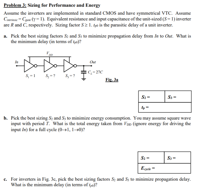
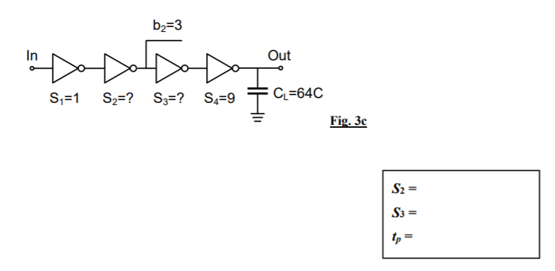
Problem 3: Sizing for Performance and Energy Assume the inverters are implemented in standard CMOS and have symmetrical VTC. Assume Cintrinsic = Cgate (r= 1). Equivalent resistance and input capacitance of the unit-sized (S= 1) inverter are R and C, respectively. Sizing factor S2 1. tpo is the parasitic delay of a unit inverter. a. Pick the best sizing factors S2 and S3 to minimize propagation delay from In to Out. What is the minimum delay (in terms of tpo)? V DD In Out C = 27C S = 1 S, = ? Sz = ? Fig. 3a S2 = S3 = tp = b. Pick the best sizing S2 and S3 to minimize energy consumption. You may assume square wave input with period T. What is the total energy taken from Vpp (ignore energy for driving the input In) for a full cycle (0-1, 1-0)? S2 = S3 = E cycle = c. For inverters in Fig. 3c, pick the best sizing factors S2 and S3 to minimize propagation delay. What is the minimum delay (in terms of tpo)? b2=3 In Out Si=1 Sz=? Sz=? Sz=? S4=9 CL=64C Fig. 3c S2 = S3 = tp =
Step by Step Solution
There are 3 Steps involved in it

Get step-by-step solutions from verified subject matter experts