

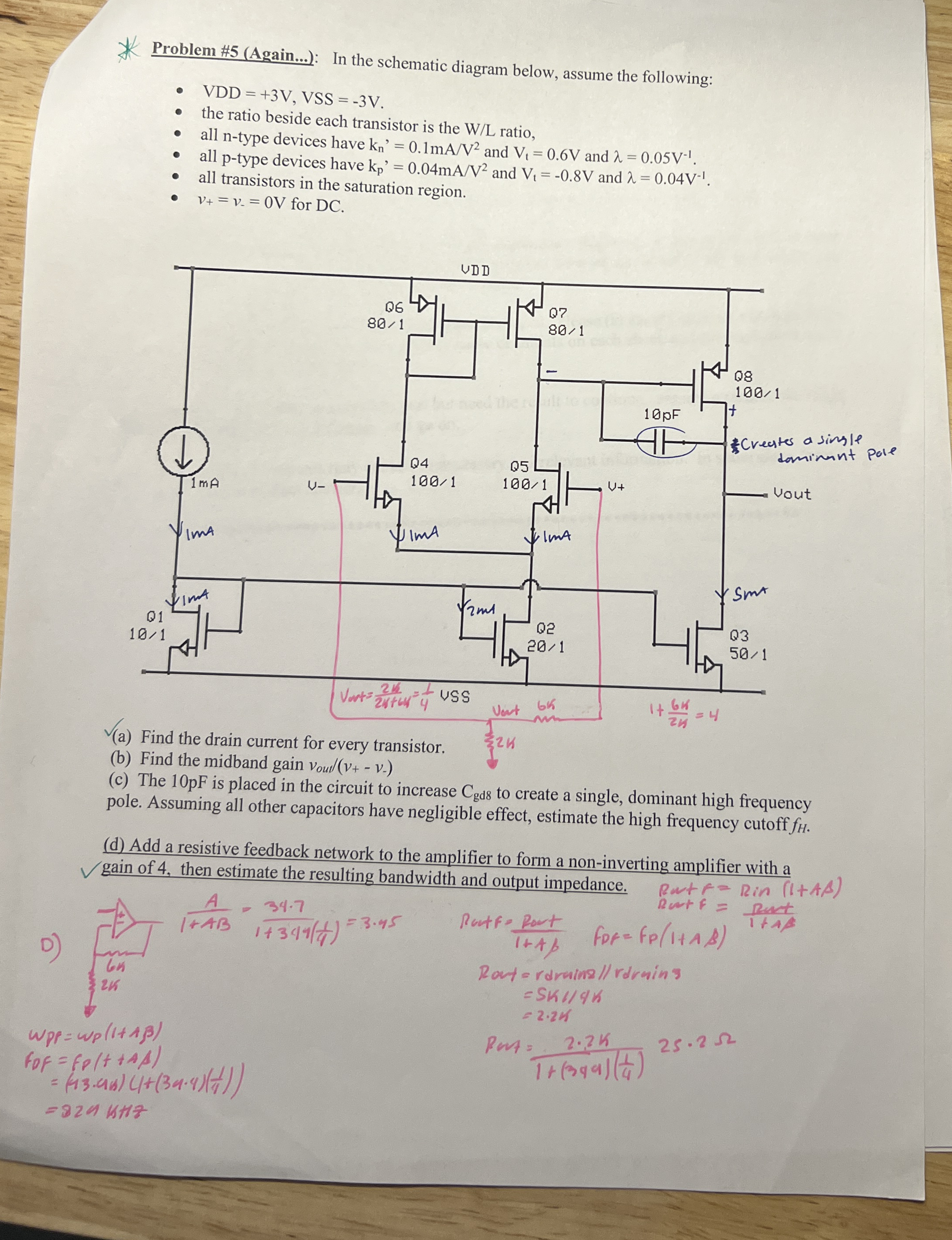
Question: Problem # 5 ( Again . . . ) : In the schematic diagram below, assume the following: V D D = + 3 V
Problem #Again: In the schematic diagram below, assume the following:
the ratio beside each transistor is the ratio,
all ntype devices have and and
all ptype devices have and and
all transistors in the saturation region.
for DC
b Find the midband gain
c The pF is placed in the circuit to increase to create a single, dominant high frequency pole. Assuming all other capacitors have negligible effect, estimate the high frequency cutoff
d Add a resistive feedback network to the amplifier to form a noninverting amplifier with a gain of then estimate the resulting bandwidth and output impedance. Rowt Rin
D
Putf
Rat rdruinedrnins
Step by Step Solution
There are 3 Steps involved in it
1 Expert Approved Answer
Step: 1 Unlock

Question Has Been Solved by an Expert!
Get step-by-step solutions from verified subject matter experts
Step: 2 Unlock
Step: 3 Unlock