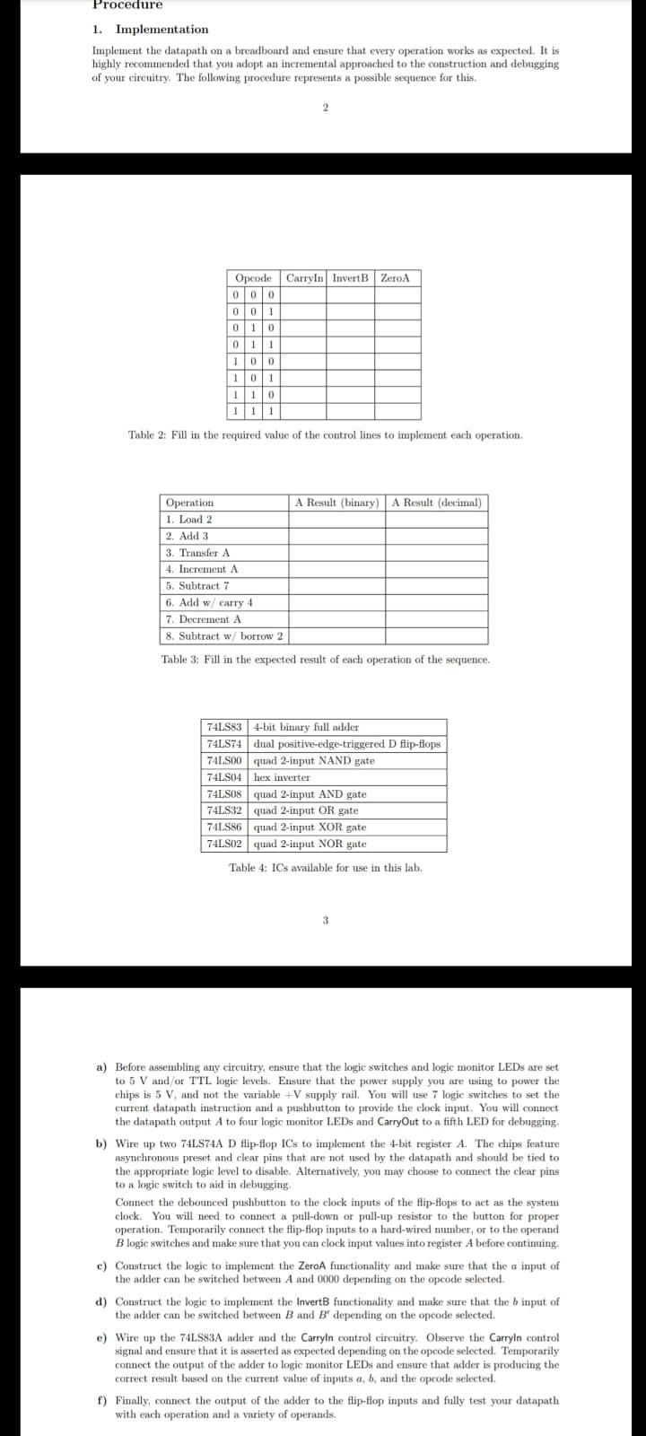
Question: Procedure 1. Implementation Implement the datapath on a breadboard and ensure that every operation works as expected. It is highly recommended that you adopt an

Procedure 1. Implementation Implement the datapath on a breadboard and ensure that every operation works as expected. It is highly recommended that you adopt an incremental approached to the construction and debugging of your circuitry. The following procedure represents a possible sequence for this, 2 Carryin InvertB Zero Opcode 000 001 0 1 0 0 1 1 0 0 1 0 1 11 11 0 1 Table 2: Fill in the required value of the control lines to implement each operation A Result (binary A Result (decimal) Operation 1. Load 2 2. Add 3 3. Transfer A 4. Increment A 5. Subtract 7 6. Add w carry 4 7. Decrement A 8. Subtract w/ borrow 2 Table 3: Fill in the expected result of each operation of the sequence. 74LS834-bit binary full adder 74LS74 dual positive-edge-triggered D flip-flops 74L.S00 quad 2-input NAND gate 741.804 hex inverter 74LSOS quad 2-input AND gate 74LS32 quad 2-input OR gate 741.586 quand 2-input XOR gate 74LS02 quad 2-input NOR gute Table 4: ICs available for use in this lab. 3 a) Before assembling any circuitry, ensure that the logic switches and logie monitor LEDs are set to 5 V and/or TTL logic levels. Ensure that the power supply you are using to power the chips is 5 V, and not the variable +V supply rail. You will use 7 logic switches to set the current datapath instruction and a pushbutton to provide the clock input. You will connect the datapath output A to four logic monitor LEDs and CarryOut to a fifth LED for debugging b) Wire up two 74LS74A D flip-flop ICs to implement the 4-bit register A. The chips feature asynchronous preset and clear pins that are not used by the datapath and should be tied to the appropriate logic level to disable. Alternatively, you may choose to connect the clear pins to a logic switch to aid in debugging Connect the debounced pushbutton to the clock inputs of the flip-flops to act as the system clock. You will need to connect a pull-down or pull-up resistor to the button for proper operation. Temporarily connect the flip-flop inputs to a hard-wired number, or to the operand B logic switches and make sure that you can clock input values into register A before continuing c) Construct the logic to implement the ZeroA functionality and make sure that the a input of the adder can be switched between A and 0000 depending on the opcode selected d) Construct the logic to implement the Inverts functionality and make sure that the b input of the adder can be switched between B and B' depending on the opcode selected. e) Wire up the 74LS83A adder and the Carryin control circuitry. Observe the Carryin control signal and ensure that it is asserted as expected depending on the opcode selected. Temporarily connect the output of the adder to logic monitor LEDs and ensure that adder is producing the correct result based on the current value of inputs a, b, and the opcode selected. f) Finally, connect the output of the adder to the flip-flop inputs and fully test your datapath with each operation and a variety of operands
Step by Step Solution
There are 3 Steps involved in it

Get step-by-step solutions from verified subject matter experts


