

Question: Provide a sequential logic design with Verilog code that displays successive digits of your ID: 0,1,2,3,4,5,6,7 on a two-pushbutton switch, 4-digit 7-segment LED display. 1.
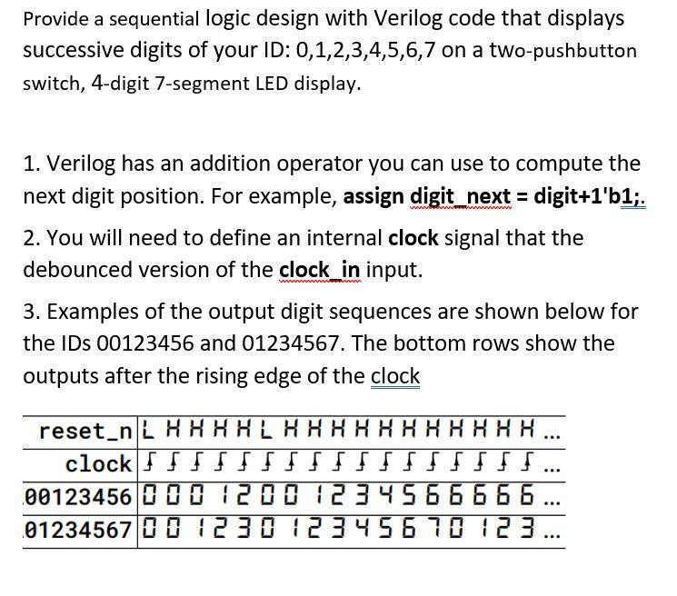
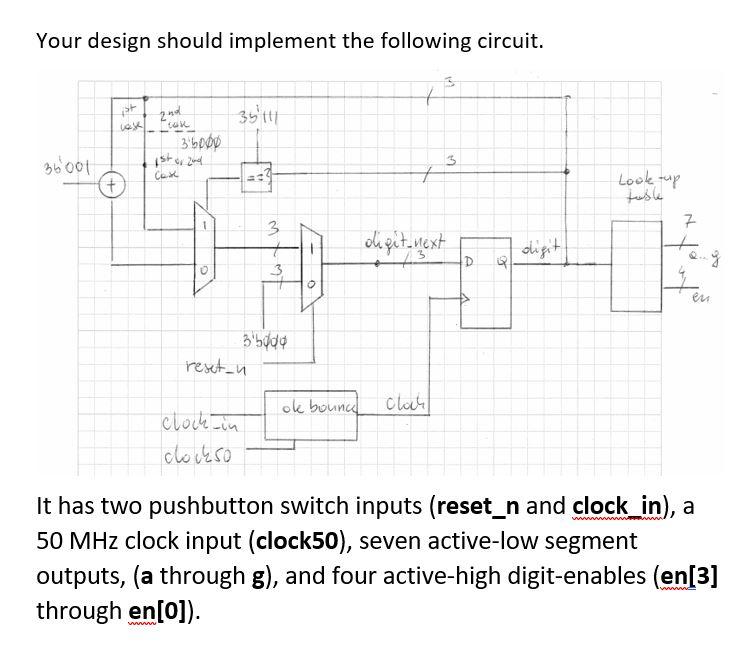
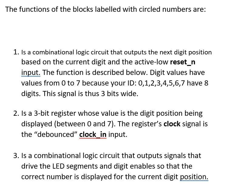
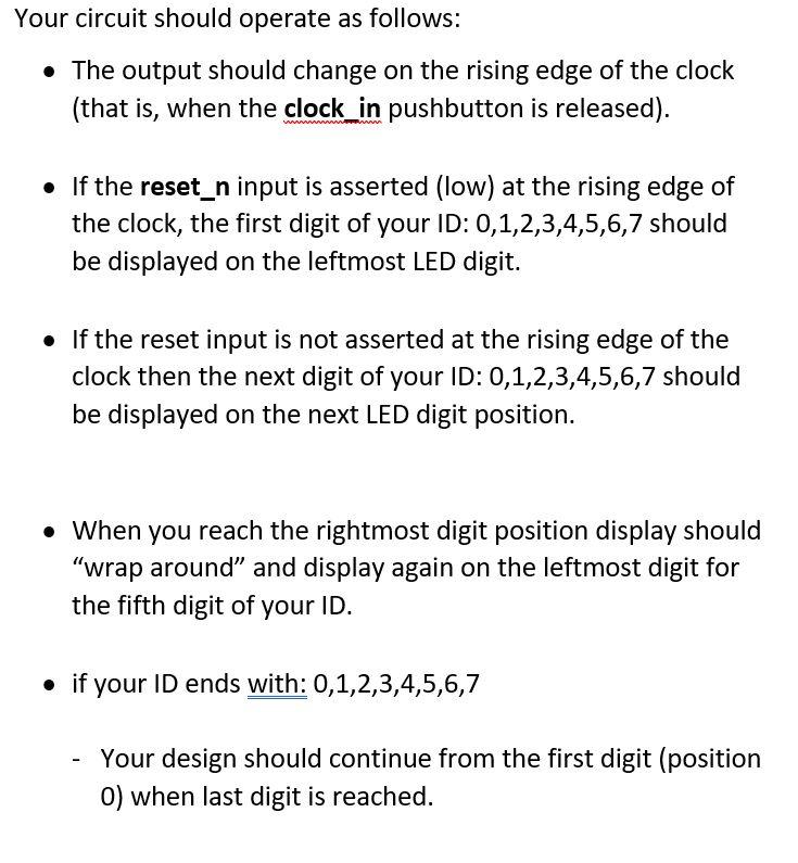
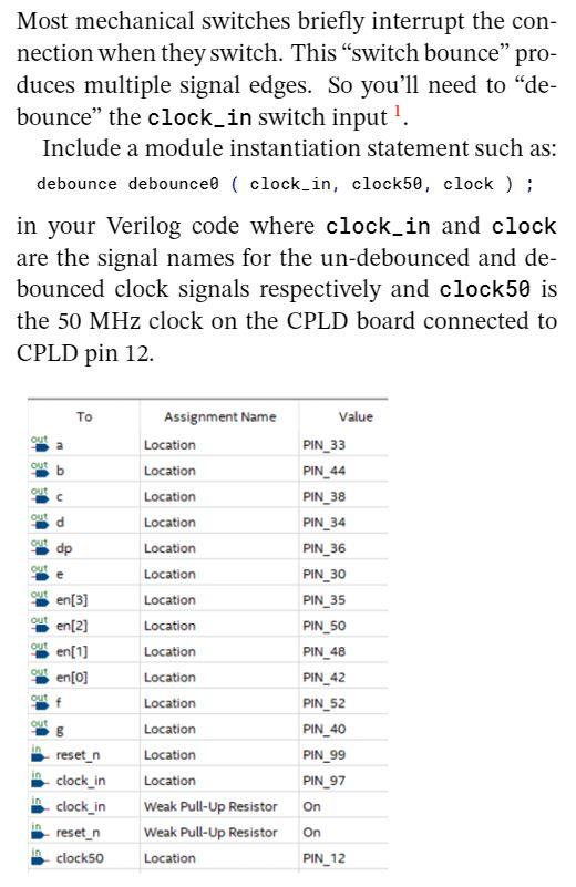
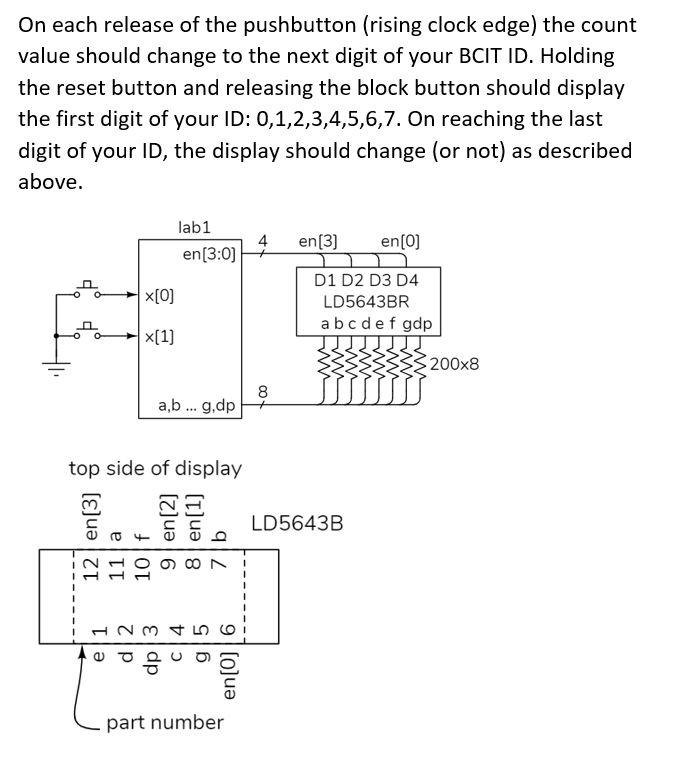
Provide a sequential logic design with Verilog code that displays successive digits of your ID: 0,1,2,3,4,5,6,7 on a two-pushbutton switch, 4-digit 7-segment LED display. 1. Verilog has an addition operator you can use to compute the next digit position. For example, assign digit_next = digit+1'b1;. 2. You will need to define an internal clock signal that the debounced version of the clock_in input. 3. Examples of the output digit sequences are shown below for the IDs 00123456 and 01234567. The bottom rows show the outputs after the rising edge of the clock reset_n LHHHHLHKKKKKKKKKK clock FIIIIIIIIIIIIIIII 00123456 0 0 0 2 0 0 1 2 3 4 5 6 6 6 6 6 01234567 0 0 1230 1 2 3 4 5 6 7 8 1 2 3 ... ... Your design should implement the following circuit. st 2nd 3511 3.500 36001 ist and CLX = 7 Look up tash 3 7 digit next digit D D 3 eu 350do restu ok bounced Cloch in clockso It has two pushbutton switch inputs (reset_n and clock_in), a 50 MHz clock input (clock50), seven active-low segment outputs, (a through g), and four active-high digit-enables (en[3] through en[0]). The functions of the blocks labelled with circled numbers are: 1. Is a combinational logic circuit that outputs the next digit position based on the current digit and the active-low reset_n input. The function is described below. Digit values have values from 0 to 7 because your ID: 0,1,2,3,4,5,6,7 have 8 digits. This signal is thus 3 bits wide. 2. Is a 3-bit register whose value is the digit position being displayed (between 0 and 7). The register's clock signal is the "debounced clock_in input. wwwwwwwwww 3. Is a combinational logic circuit that outputs signals that drive the LED segments and digit enables so that the correct number is displayed for the current digit position. Your circuit should operate as follows: The output should change on the rising edge of the clock (that is, when the clock_in pushbutton is released). If the reset_n input is asserted (low) at the rising edge of the clock, the first digit of your ID: 0,1,2,3,4,5,6,7 should be displayed on the leftmost LED digit. If the reset input is not asserted at the rising edge of the clock then the next digit of your ID: 0,1,2,3,4,5,6,7 should be displayed on the next LED digit position. When you reach the rightmost digit position display should "wrap around" and display again on the leftmost digit for the fifth digit of your ID. if your ID ends with: 0,1,2,3,4,5,6,7 Your design should continue from the first digit (position 0) when last digit is reached. Most mechanical switches briefly interrupt the con- nection when they switch. This switch bounce" pro- duces multiple signal edges. So you'll need to de- bounce the clock in switch input. Include a module instantiation statement such as: debounce debounce ( clock_in, clock50, clock ) ; in your Verilog code where clock_in and clock are the signal names for the un-debounced and de- bounced clock signals respectively and clock50 is the 50 MHz clock on the CPLD board connected to CPLD pin 12. out out out out dp en[3] en[2] Assignment Name Location Location Location Location Location Location Location Location Location Location Location Location Location Location Weak Pull-Up Resistor Weak Pull-Up Resistor Location Value PIN_33 PIN_44 PIN_38 PIN_34 PIN_36 PIN_30 PIN_35 PIN_50 PIN_48 PIN_42 PIN_52 PIN_40 PIN_99 PIN_97 On en[1] en[0] out out reset_n clock_in clock_in reset_n clock50 On PIN_12 On each release of the pushbutton (rising clock edge) the count value should change to the next digit of your BCIT ID. Holding the reset button and releasing the block button should display the first digit of your ID: 0,1,2,3,4,5,6,7. On reaching the last digit of your ID, the display should change (or not) as described above. lab1 en(3:0) 4 en (3) en(0) x[O] D1 D2 D3 D4 LD5643BR abcdefgdp X[1] 200x8 8 ab... g,dp top side of display LD5643B 12 en[3] 9 en[2] 8 en(1) 10f 7b 11 a 1 ! ! ! e 1 dp 3 C4 g5 en(O) 6 part number E888 UAB Provide a sequential logic design with Verilog code that displays successive digits of your ID: 0,1,2,3,4,5,6,7 on a two-pushbutton switch, 4-digit 7-segment LED display. 1. Verilog has an addition operator you can use to compute the next digit position. For example, assign digit_next = digit+1'b1;. 2. You will need to define an internal clock signal that the debounced version of the clock_in input. 3. Examples of the output digit sequences are shown below for the IDs 00123456 and 01234567. The bottom rows show the outputs after the rising edge of the clock reset_n LHHHHLHKKKKKKKKKK clock FIIIIIIIIIIIIIIII 00123456 0 0 0 2 0 0 1 2 3 4 5 6 6 6 6 6 01234567 0 0 1230 1 2 3 4 5 6 7 8 1 2 3 ... ... Your design should implement the following circuit. st 2nd 3511 3.500 36001 ist and CLX = 7 Look up tash 3 7 digit next digit D D 3 eu 350do restu ok bounced Cloch in clockso It has two pushbutton switch inputs (reset_n and clock_in), a 50 MHz clock input (clock50), seven active-low segment outputs, (a through g), and four active-high digit-enables (en[3] through en[0]). The functions of the blocks labelled with circled numbers are: 1. Is a combinational logic circuit that outputs the next digit position based on the current digit and the active-low reset_n input. The function is described below. Digit values have values from 0 to 7 because your ID: 0,1,2,3,4,5,6,7 have 8 digits. This signal is thus 3 bits wide. 2. Is a 3-bit register whose value is the digit position being displayed (between 0 and 7). The register's clock signal is the "debounced clock_in input. wwwwwwwwww 3. Is a combinational logic circuit that outputs signals that drive the LED segments and digit enables so that the correct number is displayed for the current digit position. Your circuit should operate as follows: The output should change on the rising edge of the clock (that is, when the clock_in pushbutton is released). If the reset_n input is asserted (low) at the rising edge of the clock, the first digit of your ID: 0,1,2,3,4,5,6,7 should be displayed on the leftmost LED digit. If the reset input is not asserted at the rising edge of the clock then the next digit of your ID: 0,1,2,3,4,5,6,7 should be displayed on the next LED digit position. When you reach the rightmost digit position display should "wrap around" and display again on the leftmost digit for the fifth digit of your ID. if your ID ends with: 0,1,2,3,4,5,6,7 Your design should continue from the first digit (position 0) when last digit is reached. Most mechanical switches briefly interrupt the con- nection when they switch. This switch bounce" pro- duces multiple signal edges. So you'll need to de- bounce the clock in switch input. Include a module instantiation statement such as: debounce debounce ( clock_in, clock50, clock ) ; in your Verilog code where clock_in and clock are the signal names for the un-debounced and de- bounced clock signals respectively and clock50 is the 50 MHz clock on the CPLD board connected to CPLD pin 12. out out out out dp en[3] en[2] Assignment Name Location Location Location Location Location Location Location Location Location Location Location Location Location Location Weak Pull-Up Resistor Weak Pull-Up Resistor Location Value PIN_33 PIN_44 PIN_38 PIN_34 PIN_36 PIN_30 PIN_35 PIN_50 PIN_48 PIN_42 PIN_52 PIN_40 PIN_99 PIN_97 On en[1] en[0] out out reset_n clock_in clock_in reset_n clock50 On PIN_12 On each release of the pushbutton (rising clock edge) the count value should change to the next digit of your BCIT ID. Holding the reset button and releasing the block button should display the first digit of your ID: 0,1,2,3,4,5,6,7. On reaching the last digit of your ID, the display should change (or not) as described above. lab1 en(3:0) 4 en (3) en(0) x[O] D1 D2 D3 D4 LD5643BR abcdefgdp X[1] 200x8 8 ab... g,dp top side of display LD5643B 12 en[3] 9 en[2] 8 en(1) 10f 7b 11 a 1 ! ! ! e 1 dp 3 C4 g5 en(O) 6 part number E888 UAB
Step by Step Solution
There are 3 Steps involved in it

Get step-by-step solutions from verified subject matter experts