

Question: PROVIDE ME A DETAILED SOLUTION AND COMPLETE SOLUTION AND DON'T COPY FROM CHATGPT IT IS OF NO USE. a . Consider the following Verilog module.
PROVIDE ME A DETAILED SOLUTION AND COMPLETE SOLUTION AND DON'T COPY FROM CHATGPT IT IS OF NO USE.
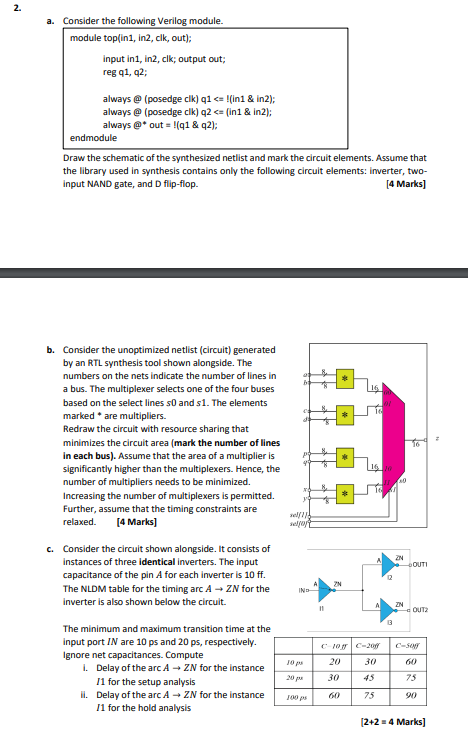
a Consider the following Verilog module.
module topin in clk out;
input in in clk; output out;
reg q q;
always @ posedge clk qin & in;
always @ posedge clk qin & in;
always @ out q & q;
endmodule
Draw the schematic of the synthesized netlist and mark the circuit elements. Assume that
the library used in synthesis contains only the following circuit elements: inverter, two
input NAND gate, and D flipflop.
b Consider the unoptimized netlist circuit generated
by an RTL synthesis tool shown alongside. The
numbers on the nets indicate the number of lines in
a bus. The multiplexer selects one of the four buses
based on the select lines s and s The elements
marked are multipliers.
Redraw the circuit with resource sharing that
minimizes the circuit area mark the number of lines
in each bus Assume that the area of a multiplier is
significantly higher than the multiplexers. Hence, the
number of multipliers needs to be minimized.
Increasing the number of multiplexers is permitted.
Further, assume that the timing constraints are
relaxed.
Marks
c Consider the circuit shown alongside. It consists of
instances of three identical inverters. The input
capacitance of the pin A for each inverter is ff
The NLDM table for the timing arc A rarr ZN for the
inverter is also shown below the circuit.
The minimum and maximum transition time at the
input port IN are ps and ps respectively.
Ignore net capacitances. Compute
i Delay of the arc A rarr ZN for the instance
I for the setup analysis
ii Delay of the arc A rarr ZN for the instance
I for the hold analysis
Marks
Step by Step Solution
There are 3 Steps involved in it
1 Expert Approved Answer
Step: 1 Unlock

Question Has Been Solved by an Expert!
Get step-by-step solutions from verified subject matter experts
Step: 2 Unlock
Step: 3 Unlock