

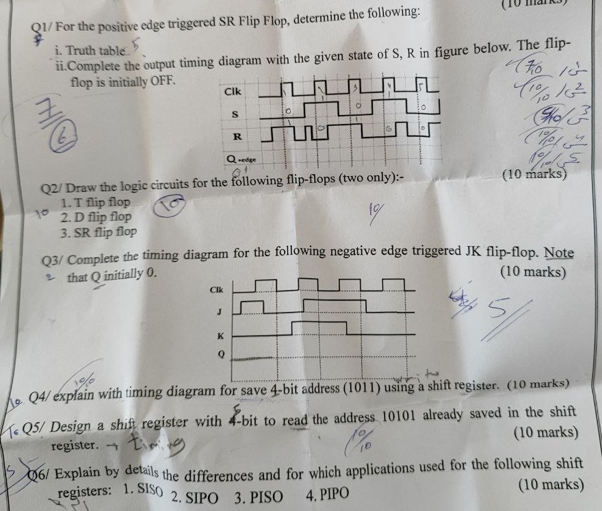
Question: Q 1 / For the positive edge triggered SR Flip Flop, determine the following: i . Truth table 5 ii . Complete the output timing
Q For the positive edge triggered SR Flip Flop, determine the following:
i Truth table
ii Complete the output timing diagram with the given state of in figure below. The flipflop is initially OFF.
Q Draw the logic circuits for the following InpHops two uny
T flip flop
D flip flop
SR flip flop
Q Complete the timing diagram for the following negative edge triggered JK flipflop. Note that initially
marks
Q explain with timing diagram for save bit address using a shift register. marks K Q Design a shift register with bit to read the address already saved in the shift register. Lisi,
marks
Q Explain by details the differences and for which applications used for the following shift registers: SISO SIPO PISO PIPO
marks solve this question
Step by Step Solution
There are 3 Steps involved in it
1 Expert Approved Answer
Step: 1 Unlock

Question Has Been Solved by an Expert!
Get step-by-step solutions from verified subject matter experts
Step: 2 Unlock
Step: 3 Unlock