

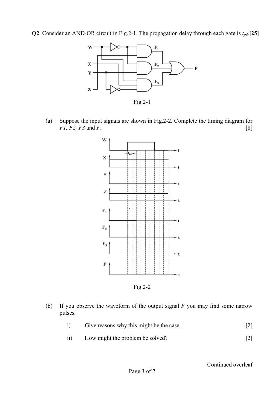
Question: Q 2 Consider an AND - OR circuit in Fig . 2 - 1 . The propagation delay through each gate is t p d
Q Consider an ANDOR circuit in Fig The propagation delay through each gate is
a Suppose the input signals are shown in Fig Complete the timing diagram for and
b If you observe the waveform of the output signal you may find some narrow pulses.
i Give reasons why this might be the case.
ii How might the problem be solved?
Continued overleaf
Page of
Step by Step Solution
There are 3 Steps involved in it
1 Expert Approved Answer
Step: 1 Unlock

Question Has Been Solved by an Expert!
Get step-by-step solutions from verified subject matter experts
Step: 2 Unlock
Step: 3 Unlock