

Question: Question 1: Implement the following function using a single CMOS gate. Assume inputs and their complement are available. 1. F1 = (A+B+C)D 2. F2 =
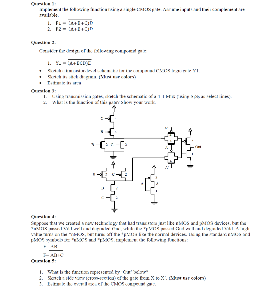
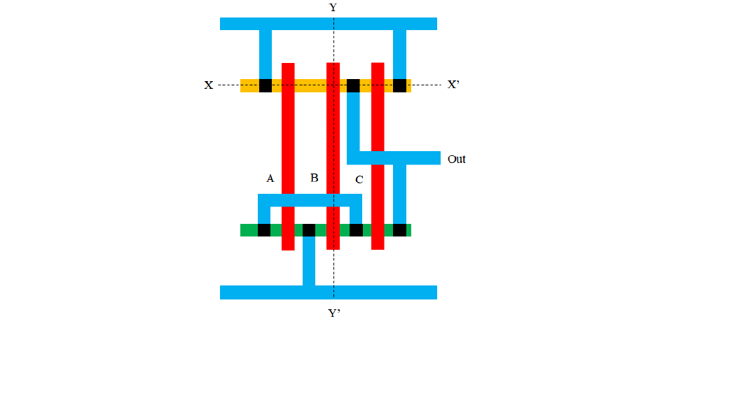
Question 1: Implement the following function using a single CMOS gate. Assume inputs and their complement are available. 1. F1 = (A+B+C)D 2. F2 = (A+B+C)D Question 2: Consider the design of the following compound gate: 1. Y1 = (A+BCDE Sketch a transistor-level schematic for the compound CMOS logic gate Y1. Sketch its stick diagram. (Must use colors) Estimate its area Question 3: 1. Using transmission gates, sketch the schematic of a 4-1 Mux (using Si So as select lines). 2. What is the function of this gate? Show your work. c 4 B 4 B C Out A B B Question 4: Suppose that we created a new technology that had transistors just like nMOS and PMOS devices, but the *nMOS passed Vdd well and degraded Gnd, while the "pMOS passed Gnd well and degraded Vdd. A high value turns on the *nMOS, but turns off the *pMOS like the normal devices. Using the standard nMOS and PMOS symbols for *nMOS and *pMOS, implement the following functions: F= AB F= AB+C Question 5: 1 What is the function represented by 'Out' below? Sketch a side view (cross-section of the gate from X to X'. (Must use colors) 3. Estimate the overall area of the CMOS compound gate. 2 Out A B
Step by Step Solution
There are 3 Steps involved in it

Get step-by-step solutions from verified subject matter experts