Question: Question 1 ( total 8 8 marks , and 8 bonus marks ) A certain door lock system uses a keypad with 1 2 buttons
Question total marks and bonus marks
A certain door lock system uses a keypad with buttonsto and #and uses rowcolumn encoding by assigning bits to row number, and bits to column number, as follows:
Keypad : #
Truth table: A B C D Button
#
The keyboard generates a clock signal every time a button is pressed so the connecting circuitry can sample the values of signals ABCand DYou are going to design a circuit that recognises the sequence # as an unrelated note, the number happens to be the Kaprekar's constantand have decided to recognise the four sequences separately, then AND them together to form the final result.
amarksThe four recognisers have the same number of states. How many states are there?
bmarksWhat are the four sequences to be recognised?
cmarksDraw a Mealy model state diagram for each recogniser, naming the states AAdots for the As sequence recogniser, BBdots for Bsand so onA recogniser should reset to its initial state on detection of wrong input.
dmarksSuppose the four sequence recognisers for ABC and D are modules named RARBRC and RD respectively, drawn as rectangular boxes with input D clock Clk use a little triangle like that of a flipflop to represent itand output QDraw the circuit schematic diagram that makes use of these modules and logic gatesthat implement the sequence recognition function. The circuit takes inputs ABCDand Clock from the keypad module, and outputs R whose logic is when the sequence is recognised, and otherwise
emarksDraw the symbolic state table for module RAThe columns should be the current symbolic state AAetcthe input Athe next symbolic state, and the output of the module, QA
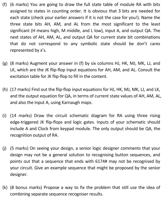
f marks You are going to draw the full state table of module RA with bits assigned to states in counting order. It is obvious that bits are needed for each state check your earlier answers if it is not the case for you! Name the three state bits AHAM and AL from the most significant to the least significant H means high, M middle, and L low input A and output QA The next states of AHAMAL and output QA for current state bit combinations that do not correspond to any symbolic state should be don't cares represented by x s
g marks Augment your answer in f by six columns HJ HK MJ MK L and LK which are the JK flipflop input equations for AH AM and AL Consult the excitation table for JK flipflop to fill in the content.
h marks Find out the flipflop input equations for HJ HK MJ MK LJ and LK and the output equation for QA in terms of current state values of AHAMAL and also the input A using Karnaugh maps.
i marks Draw the circuit schematic diagram for RA using three rising
edgetriggered JK flipflops and logic gates. Inputs of your schematic should include A and Clock from keypad module. The only output should be QA the recognition output of RA
j marks On seeing your design, a senior logic designer comments that your design may not be a general solution to recognising button sequences, and points out that a sequence that ends with # may not be recognised by your circuit. Give an example sequence that might be proposed by the senior designer.
k bonus marks Propose a way to fix the problem that still use the idea of combining separate sequence recogniser results.

Step by Step Solution
There are 3 Steps involved in it
1 Expert Approved Answer
Step: 1 Unlock


Question Has Been Solved by an Expert!
Get step-by-step solutions from verified subject matter experts
Step: 2 Unlock
Step: 3 Unlock


