

Question: Question 4 ( 3 + 3 + 3 marks ) The following FSM has been designed with an initial clock period is 9 ns .
Question marks
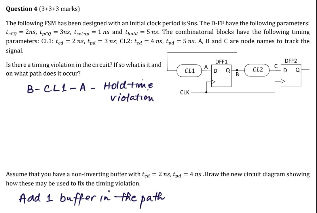
The following FSM has been designed with an initial clock period is ns The DFF have the following parameters: and The combinatorial blocks have the following timing parameters: CL: ; CL: A B and C are node names to track the signal.
Is there a timing violation in the circuit? If so what is it and on what path does it occur?
BCLA Holdtime
violation
Assume that you have a noninverting buffer with Draw the new circuit diagram showing how these may be used to fix the timing violation.
Add buffer in the path
Step by Step Solution
There are 3 Steps involved in it
1 Expert Approved Answer
Step: 1 Unlock

Question Has Been Solved by an Expert!
Get step-by-step solutions from verified subject matter experts
Step: 2 Unlock
Step: 3 Unlock