

Question: Question 6 ( 1 0 points ) Design the controller for the paraller to serial conversion of 4 - bit data using the shift register
Question points
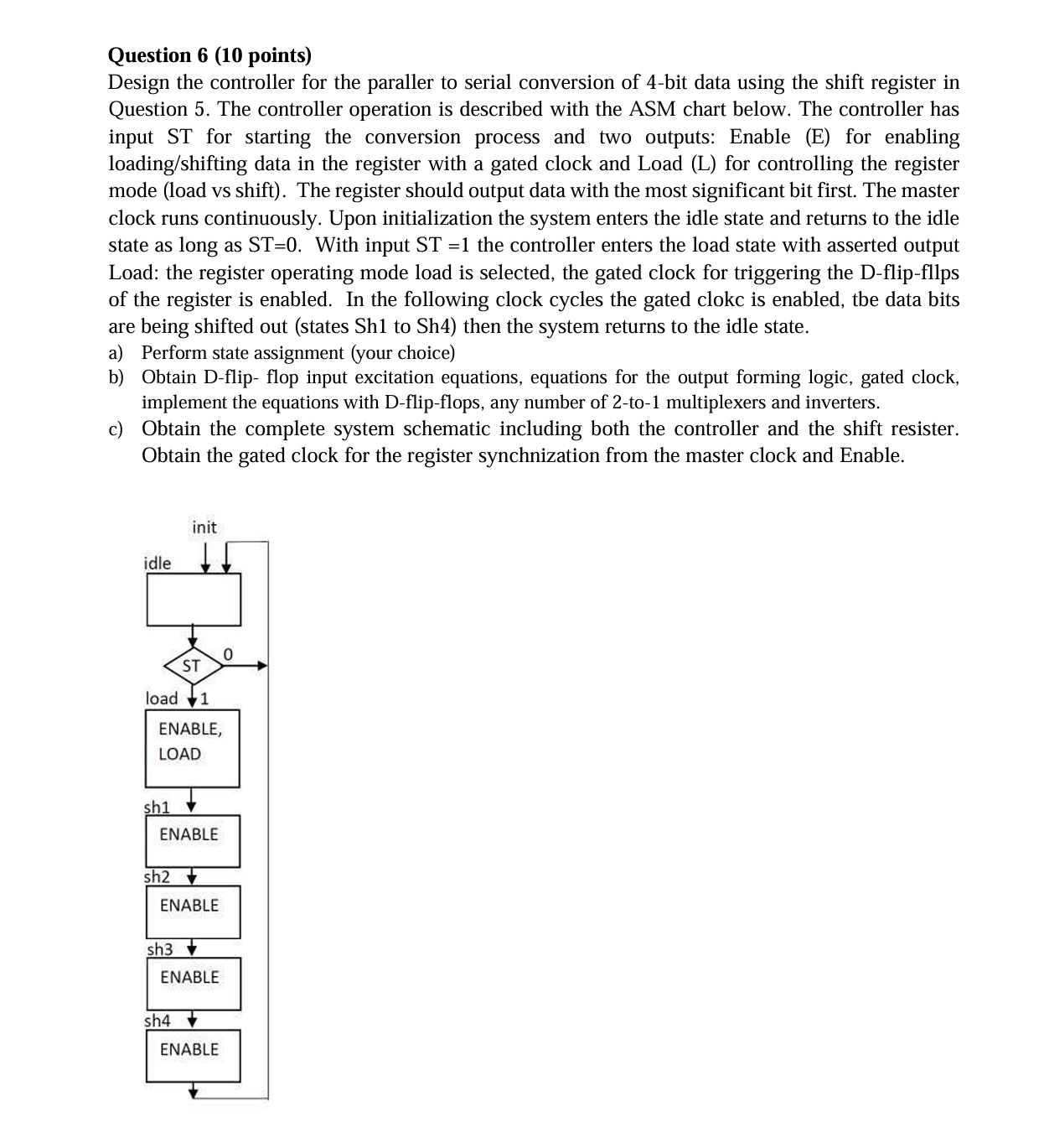
Design the controller for the paraller to serial conversion of bit data using the shift register in Question The controller operation is described with the ASM chart below. The controller has input ST for starting the conversion process and two outputs: Enable E for enabling loadingshifting data in the register with a gated clock and Load L for controlling the register mode load vs shift The register should output data with the most significant bit first. The master clock runs continuously. Upon initialization the system enters the idle state and returns to the idle state as long as mathrmST With input mathrmST the controller enters the load state with asserted output Load: the register operating mode load is selected, the gated clock for triggering the Dflipfllps of the register is enabled. In the following clock cycles the gated clokc is enabled, tbe data bits are being shifted out states Sh to Sh then the system returns to the idle state.
a Perform state assignment your choice
b Obtain Dflip flop input excitation equations, equations for the output forming logic, gated clock, implement the equations with Dflipflops, any number of to multiplexers and inverters.
c Obtain the complete system schematic including both the controller and the shift resister. Obtain the gated clock for the register synchnization from the master clock and Enable.
Step by Step Solution
There are 3 Steps involved in it
1 Expert Approved Answer
Step: 1 Unlock

Question Has Been Solved by an Expert!
Get step-by-step solutions from verified subject matter experts
Step: 2 Unlock
Step: 3 Unlock