

Question: Question 7 ( 1 2 marks ) Consider the following circuit. The input NAND has an input capacitance of 1 0 units. The output capacitance
Question marks
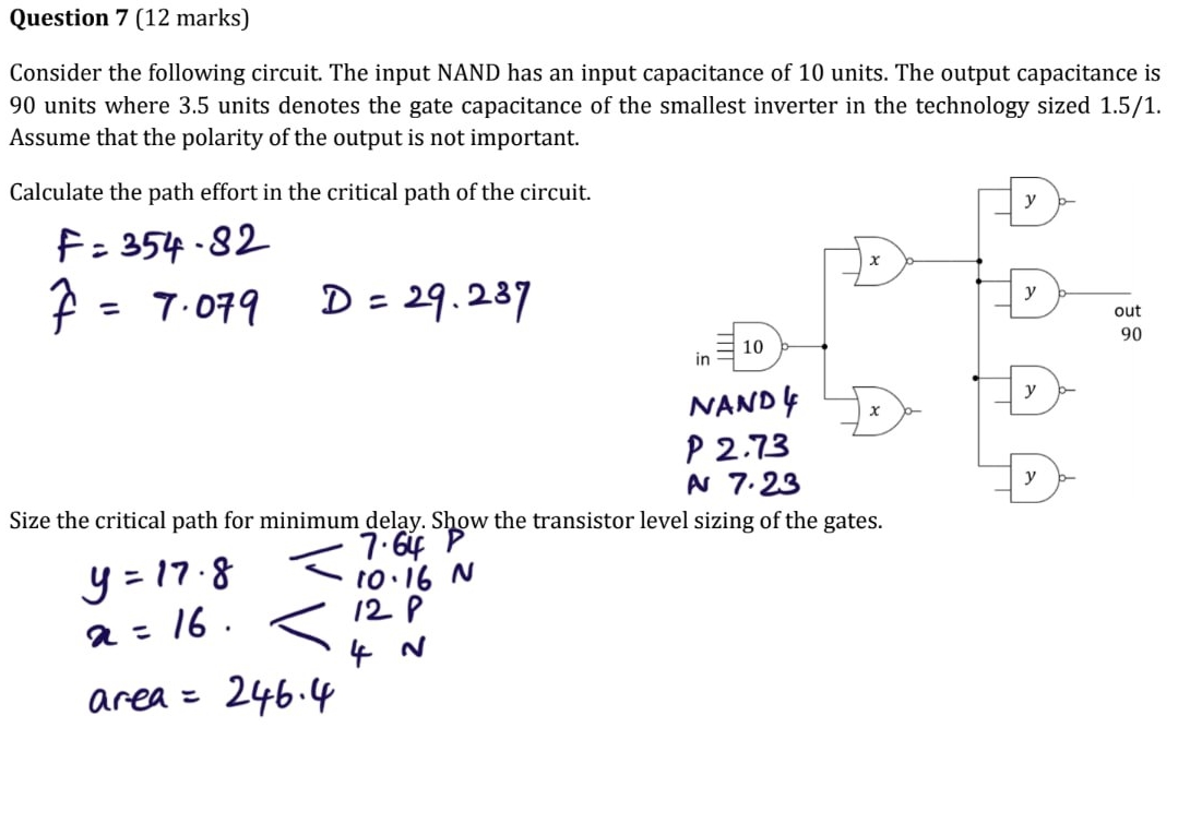
Consider the following circuit. The input NAND has an input capacitance of units. The output capacitance is units where units denotes the gate capacitance of the smallest inverter in the technology sized Assume that the polarity of the output is not important.
Calculate the path effort in the critical path of the circuit.
hat
Size the critical path for minimum delay. Show the transistor le
Step by Step Solution
There are 3 Steps involved in it
1 Expert Approved Answer
Step: 1 Unlock

Question Has Been Solved by an Expert!
Get step-by-step solutions from verified subject matter experts
Step: 2 Unlock
Step: 3 Unlock