

Question: Question A2 We will design a digital circuit, based on the following truth table, which has three inputs, A, B, and C, and two outputs
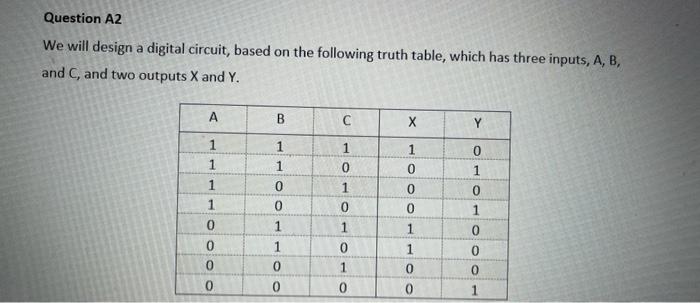
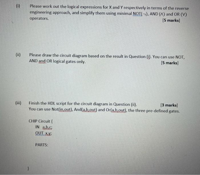
Question A2 We will design a digital circuit, based on the following truth table, which has three inputs, A, B, and C, and two outputs X and Y. A B Y 1 1 1 0 0 0 1 0 0 1 1 1 1 0 0 0 0 0 1 0 1 0 0 0 0 1 1 1 0 1 0 1 0 0 0 1 0 0 (i) Please work out the logical expressions for X and Y respectively in terms of the reverse engineering approach, and simplify them using minimal NOTI), AND () and OR (V) operators. [5 marks] Please draw the circuit diagram based on the result in Question (O). You can use NOT, AND and OR logical gates only. [5 marks] Finish the HDL script for the circuit diagram in Question (ii). [3 marks You can use Not(in,out), Anda.b.out) and Orla.b.out), the three pre-defined gates. CHIP Circuit IN abs OUT. XX PARTS
Step by Step Solution
There are 3 Steps involved in it

Get step-by-step solutions from verified subject matter experts