

Question: Question: Design of ReconfigurableCache Memory Using Verilog HDL. Write a report on thispaper which contains 4 parts ( basic idea, advantages,implementation, challenges) Report is given
Question: Design of ReconfigurableCache Memory Using Verilog HDL. Write a report on thispaper which contains 4 parts ( basic idea, advantages,implementation, challenges)
Report is given below
![A[28, 19] Tag A[5, 0] The address bits of the Direct Cache Memory is shown in the Fig.2. Cache Index Offset](https://dsd5zvtm8ll6.cloudfront.net/questions/2023/12/657feb506b759_128657feb5065ad9.jpg)
![A[28] Tag bits Decoder Decoder A[18] A[17] 2-way Cache Memory Set Selection Two-way cache memory architecture](https://dsd5zvtm8ll6.cloudfront.net/questions/2023/12/657feb514f685_129657feb514bc4d.jpg)
![Set memory is selected using CPU address bits [18:17] shown in Table 2. A[28, 17] Tag Set Index Fig. 7: Four](https://dsd5zvtm8ll6.cloudfront.net/questions/2023/12/657feb5218e47_130657feb5214ebf.jpg)
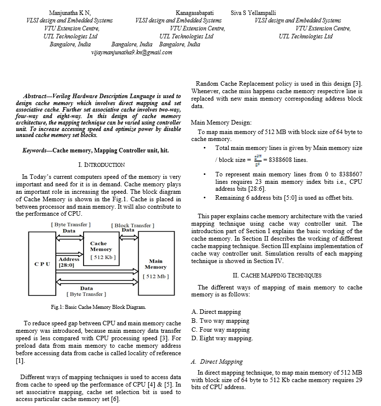
Manjunatha K N, VLSI design and Embedded Systems VTU Extension Centre, UTL Technologies Ltd Bangalore, India Abstract-Verilog Hardware Description Language is used to design cache memory which involves direct mapping and set associative cache. Further set associative cache involves two-way, four-way and eight-way. In this design of cache memory architecture, the mapping technique can be varied using controller unit. To increase accessing speed and optimize power by disable unused cache memory set blocks. CPU Kanagasabapati VLSI design and Embedded Systems VTU Extension Centre, UTL Technologies Ltd Bangalore, India Bangalore, India vijaymanjunatha9.kn@gmail.com Keywords Cache memory, Mapping Controller unit, hit. I. INTRODUCTION In Today's current computers speed of the memory is very important and need for it is in demand. Cache memory plays an important role in increasing the speed. The block diagram of Cache Memory is shown in the Fig.1. Cache is placed in between processor and main memory. It will also contribute to the performance of CPU. [Byte Transfer] Data Address [28:0] [Block Transfer ] Data Cache Memory [512 Kb] Main Memory [512 Mb] Data [Byte Transfer] Fig.1: Basic Cache Memory Block Diagram. To reduce speed gap between CPU and main memory cache memory was introduced, because main memory data transfer speed is less compared with CPU processing speed [3]. For preload data from main memory to cache memory address before accessing data from cache is called locality of reference [1]. Different ways of mapping techniques is used to access data from cache to speed up the performance of CPU [4] & [5]. In set associative mapping, cache set selection bit is used to access particular cache memory set [6]. Siva S Yellampalli VLSI design and Embedded Systems VTU Extension Centre, UTL Technologies Ltd Random Cache Replacement policy is used in this design [3]. Whenever, cache miss happens cache memory respective line is replaced with new main memory corresponding address block data. Main Memory Design: To map main memory of 512 MB with block size of 64 byte to cache memory. Total main memory lines is given by Main memory size /block size = = 8388608 lines. To represent main memory lines from 0 to 8388607 lines requires 23 main memory index bits i.e., CPU address bits [28:6]. Remaining 6 address bits [5:0] is used as offset bits. This paper explains cache memory architecture with the varied mapping technique using cache way controller unit. The introduction part of Section I explains the basic working of the cache memory. In Section II describes the working of different cache mapping technique. Section III explains implementation of cache way controller unit. Simulation results of each mapping technique is showed in Section IV. A. Direct mapping B. Two way mapping C. Four way mapping D. Eight way mapping. II. CACHE MAPPING TECHNIQUES The different ways of mapping of main memory to cache memory is as follows: A. Direct Mapping In direct mapping technique, to map main memory of 512 MB with block size of 64 byte to 512 Kb cache memory requires 29 bits of CPU address.
Step by Step Solution
3.39 Rating (149 Votes )
There are 3 Steps involved in it
Design of Reconfigurable Cache Memory Using Verilog HDL Basic Idea The paper discusses the design and implementation of a reconfigurable cache memory using Verilog HDL Hardware Description Language Th... View full answer

Get step-by-step solutions from verified subject matter experts