

Question: QUESTION ONE a ) Draw a functional block diagram and construet the compressed function table of the 7 4 LS 1 3 8 chip whic
QUESTION ONE
a Draw a functional block diagram and construet the compressed function table of the LS chip whic is a to decoder with low active outputs and three enable controls, two of them low active enbar anc enbar and one high active en
b Write down the complete and compact VDHL behavioural description of the chip including an entity header and architecture body. Assume a total propagation delay through the chip to the outputs of ns
c The WAIT statement in VHDL can have up to three clauses as given in the following BNF rules:
waitstatement :: WAIT sensitivityclause
conditionclause
timeoutclause ;
sensitivityclause :: ON sensitivitylist
conditionclause :: UNTIL booleanexpression
timeoutclause :: FOR timeexpression
Explain the semantics of the statement starting with the WAIT statement without any of the clauses, through all the combinations of included clauses to one which includes all the three clauses.
QUESTION TWO
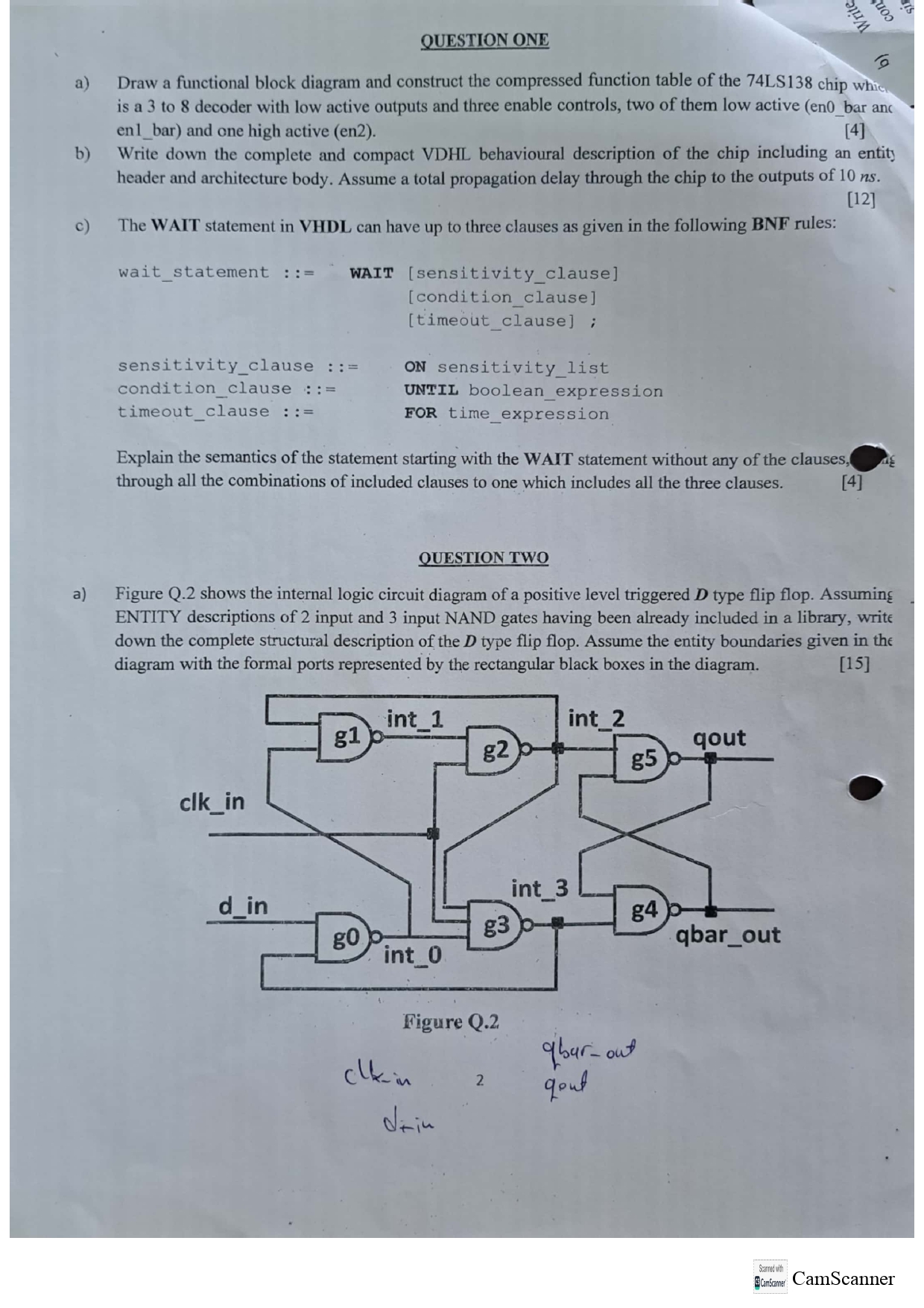
a Figure Q shows the internal logic circuit diagram of a positive level triggered boldsymbolD type flip flop. Assumin ENTITY descriptions of input and input NAND gates having been already included in a library, write down the complete structural description of the boldsymbolD type flip flop. Assume the entity boundaries given in the diagram with the formal ports represented by the rectangular black boxes in the diagram.
Step by Step Solution
There are 3 Steps involved in it
1 Expert Approved Answer
Step: 1 Unlock

Question Has Been Solved by an Expert!
Get step-by-step solutions from verified subject matter experts
Step: 2 Unlock
Step: 3 Unlock