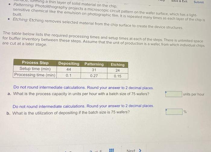
Question: Save & Exit Submit Ping a thin layer of solid material on the chip. Patterning: Photolithography projects a microscopic circuit pattern on the water surface,

Save & Exit Submit Ping a thin layer of solid
Save & Exit Submit Ping a thin layer of solid material on the chip. Patterning: Photolithography projects a microscopic circuit pattern on the water surface, which has a light- sensitive chemical like the emulsion on photographic film. It is repeated many times as each layer of the chip is built Etching: Etching removes selected material from the chip surface to create the device structures. The table below lists the required processing times and setup times at each of the steps. There is unlimited space for buffer inventory between these steps. Assume that the unit of production is a wafer, from which individual chips are cut at a later stage. Process Step Setup time (min) Processing time (min) Depositing Patterning 44 31 0.1 0.27 Etching 24 0.15 Do not round intermediate calculations, Round your answer to 2 decimal places. a. What is the process capacity in units per hour with a batch size of 75 wafers? units per hour Do not round intermediate calculations. Round your answer to 2 decimal places. b. What is the utilization of depositing if the batch size is 75 wafers? % Next

Step by Step Solution

There are 3 Steps involved in it

1 Expert Approved Answer
Step: 1 Unlock blur-text-image
Question Has Been Solved by an Expert!

Get step-by-step solutions from verified subject matter experts

Step: 2 Unlock
Step: 3 Unlock

Students Have Also Explored These Related General Management Questions!