

Question: SOLID STATE ELECTRONICS 1. Metal/semiconductor junctions Ideally, there exists either an energy barrier for electrons or one for holes? One can find the barrier height
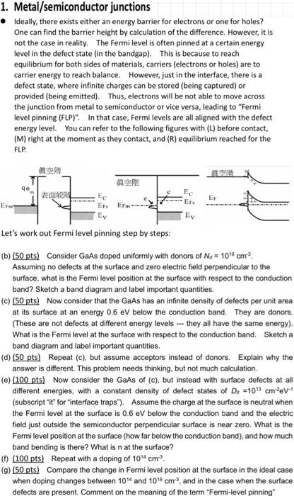
1. Metal/semiconductor junctions Ideally, there exists either an energy barrier for electrons or one for holes? One can find the barrier height by calculation of the difference. However, it is not the case in reality. The Fermi level is often pinned at a certain energy level in the defect state (in the bandgap). This is because to reach equilibrium for both sides of materials, carriers (electrons or holes) are to carrier energy to reach balance. However, just in the interface, there is a defect state, where infinite charges can be stored (being captured) or provided (being emitted). Thus, electrons will be not able to move across the junction from metal to semiconductor or vice versa, leading to "Fermi level pinning (FLP)". In that case, Fermi levels are all aligned with the defect energy level. You can refer to the following figures with (L) before contact, (M) right at the moment as they contact, and ( R ) equilibrium reached for the FLP. Let's work out Fermi level pinning step by steps: (b) (50 pts) Consider GaAs doped uniformly with donors of Nd=1016cm3. Assuming no defects at the surface and zero electric field perpendicular to the surface, what is the Fermi level position at the surface with respect to the conduction band? Sketch a band diagram and label important quantities. (c) 50 pts) Now consider that the GaAs has an infinite density of defects per unit area at its surface at an energy 0.6eV below the conduction band. They are donors. (These are not defects at different energy levels -- they all have the same energy). What is the Fermi level at the surface with respect to the conduction band. Sketch a band diagram and label important quantities. (d) 50 pts) Repeat (c), but assume acceptors instead of donors. Explain why the answer is different. This problem needs thinking, but not much calculation. (e) (100 pts) Now consider the GaAs of (c), but instead with surface defects at all different energies, with a constant density of defect states of Dfr=1013cm2eV1 (subscript "it" for "interface traps"). Assume the charge at the surface is neutral when the Fermi level at the surface is 0.6eV below the conduction band and the electric field just outside the semiconductor perpendicular surface is near zero. What is the Fermi level position at the surface (how far below the conduction band), and how much band bending is there? What is n at the surface? (f) (100 pts) Repeat with a doping of 1014cm3. (g) 50 pts) Compare the change in Fermi level position at the surface in the ideal case when doping changes between 1014 and 1016cm3, and in the case when the surface
Step by Step Solution
There are 3 Steps involved in it
Sure lets work through the questions step by step b Calculate the Fermi Level for GaAs with ND 1016 textcm3 1 Understand the Problem You have GaAs dop... View full answer

Get step-by-step solutions from verified subject matter experts