

Question: solve both parts. *****PLEASE see the reference table below to answer the questions. ********** REFERNCE TABLE Question 3 (a) Complete the code fragment below to
solve both parts.
*****PLEASE see the reference table below to answer the questions. **********
REFERNCE TABLE
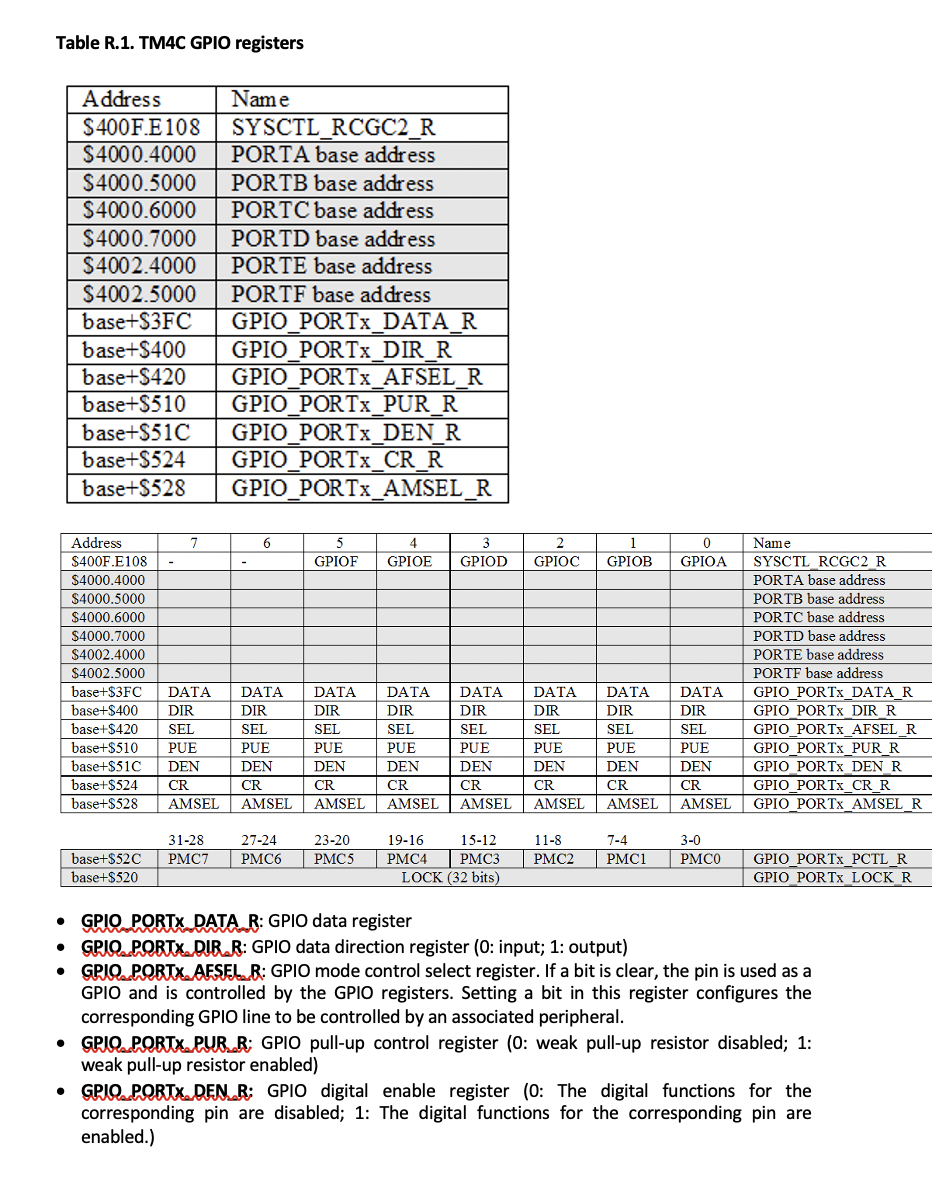
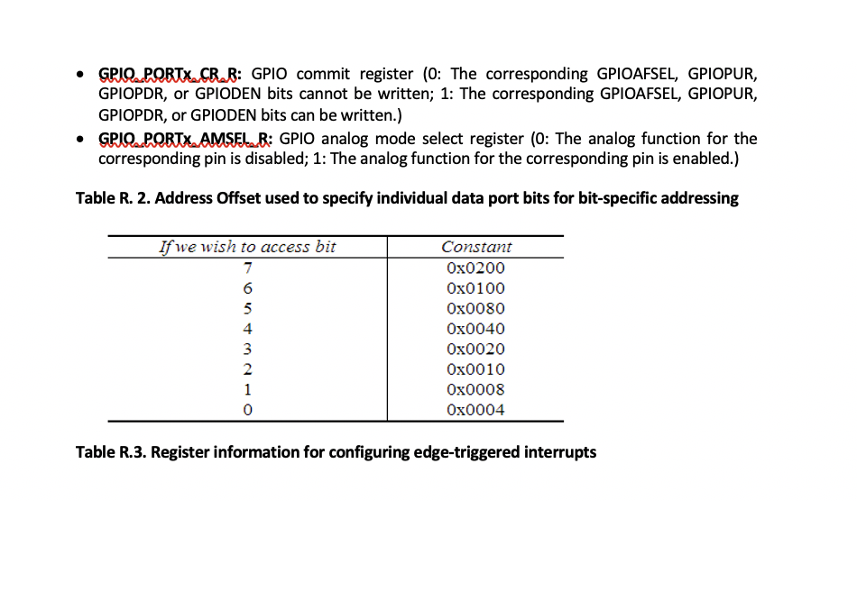
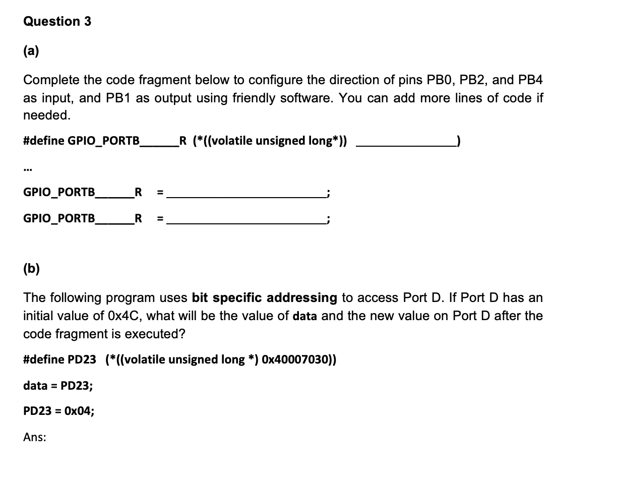
Question 3 (a) Complete the code fragment below to configure the direction of pins PBO, PB2, and PB4 as input, and PB1 as output using friendly software. You can add more lines of code if needed. #define GPIO_PORTB_ LR (*((volatile unsigned long*)) GPIO_PORTB R GPIO_PORTB R (b) The following program uses bit specific addressing to access Port D. If Port D has an initial value of 0x4C, what will be the value of data and the new value on Port D after the code fragment is executed? #define PD23 (*((volatile unsigned long *) 0x40007030)) data = PD23; PD23 = Ox04; Ans: Table R.1. TM4C GPIO registers Address $400F.E 108 $4000.4000 $4000.5000 S4000.6000 $4000.7000 S4002.4000 $4002.5000 base+S3FC base+S400 base+S420 base+S510 base+S510 base+S524 base+S528 Name SYSCTL_RCGC2_R PORTA base address PORTB base address PORTC base address PORTD base address PORTE base address PORTF base address GPIO PORTx_DATA_R GPIO_PORTx_DIR_R GPIO_PORTX_AFSEL_R GPIO_PORTx_PUR_R GPIO PORTx DEN R GPIO_PORTx_CR R GPIO_PORTX_AMSEL_R 7 6 5 GPIOF 4 GPIOE 3 GPIOD 2 GPIOC 1 GPIOB 0 GPIOA Address $400F.E108 $4000.4000 $4000.5000 $4000.6000 $4000.7000 $4002.4000 $4002.5000 base+$3FC base+$400 base+$420 base+$510 base+$510 base+$524 base+$528 Name SYSCTL_RCGC2 R PORTA base address PORTB base address PORTC base address PORTD base address PORTE base address PORTF base address GPIO_PORTx_DATA_R GPIO PORTX DIR R GPIO PORTX AFSEL R GPIO_PORTX_PUR_R GPIO PORTX DEN R GPIO_PORTx_CR_R GPIO PORTX_AMSEL_R DATA DIR SEL PUE DEN CR AMSEL DATA DIR SEL PUE DEN CR AMSEL DATA DIR SEL PUE DEN CR AMSEL DATA DIR SEL PUE DEN CR AMSEL DATA DIR SEL PUE DEN CR AMSEL DATA DIR SEL PUE DEN CR AMSEL DATA DIR SEL PUE DEN CR AMSEL DATA DIR SEL PUE DEN CR AMSEL 31-28 PMC7 27-24 PMC6 23-20 PMC5 19-16 15-12 PMC4 PMC3 LOCK (32 bits) 11-8 PMC2 7-4 PMC1 3-0 PMCO base+$520 base+$520 GPIO_PORTx_PCTL_R GPIO PORTx_LOCKR GPIO PORTX DATA R: GPIO data register GPIO PORTX.DIR.R: GPIO data direction register (C: input; 1: output) GPIO PORTX. AFSELR: GPIO mode control select register. If a bit is clear, the pin is used as a GPIO and is controlled by the GPIO registers. Setting a bit in this register configures the corresponding GPIO line to be controlled by an associated peripheral. GPIO PORTX.PURR: GPIO pull-up control register (0: weak pull-up resistor disabled; 1: weak pull-up resistor enabled) GPIO.PORTX, DENR: GPIO digital enable register (0: The digital functions for the corresponding pin are disabled; 1: The digital functions for the corresponding pin are enabled.) GPIO PORTX. CRR: GPIO commit register (0: The corresponding GPIOAFSEL, GPIOPUR, GPIOPDR, or GPIODEN bits cannot be written; 1: The corresponding GPIOAFSEL, GPIOPUR, GPIOPDR, or GPIODEN bits can be written.) GPIO PORTX.AMSELUR: GPIO analog mode select register (0: The analog function for the corresponding pin is disabled; 1: The analog function for the corresponding pin is enabled.) Table R. 2. Address Offset used to specify individual data port bits for bit-specific addressing If we wish to access bit 7 6 5 4. 3 2 1 Constant Ox0200 Ox0100 Ox0080 Ox0040 Ox0020 Ox0010 Ox0008 Ox0004 Table R.3. Register information for configuring edge-triggered interrupts Question 3 (a) Complete the code fragment below to configure the direction of pins PBO, PB2, and PB4 as input, and PB1 as output using friendly software. You can add more lines of code if needed. #define GPIO_PORTB_ LR (*((volatile unsigned long*)) GPIO_PORTB R GPIO_PORTB R (b) The following program uses bit specific addressing to access Port D. If Port D has an initial value of 0x4C, what will be the value of data and the new value on Port D after the code fragment is executed? #define PD23 (*((volatile unsigned long *) 0x40007030)) data = PD23; PD23 = Ox04; Ans: Table R.1. TM4C GPIO registers Address $400F.E 108 $4000.4000 $4000.5000 S4000.6000 $4000.7000 S4002.4000 $4002.5000 base+S3FC base+S400 base+S420 base+S510 base+S510 base+S524 base+S528 Name SYSCTL_RCGC2_R PORTA base address PORTB base address PORTC base address PORTD base address PORTE base address PORTF base address GPIO PORTx_DATA_R GPIO_PORTx_DIR_R GPIO_PORTX_AFSEL_R GPIO_PORTx_PUR_R GPIO PORTx DEN R GPIO_PORTx_CR R GPIO_PORTX_AMSEL_R 7 6 5 GPIOF 4 GPIOE 3 GPIOD 2 GPIOC 1 GPIOB 0 GPIOA Address $400F.E108 $4000.4000 $4000.5000 $4000.6000 $4000.7000 $4002.4000 $4002.5000 base+$3FC base+$400 base+$420 base+$510 base+$510 base+$524 base+$528 Name SYSCTL_RCGC2 R PORTA base address PORTB base address PORTC base address PORTD base address PORTE base address PORTF base address GPIO_PORTx_DATA_R GPIO PORTX DIR R GPIO PORTX AFSEL R GPIO_PORTX_PUR_R GPIO PORTX DEN R GPIO_PORTx_CR_R GPIO PORTX_AMSEL_R DATA DIR SEL PUE DEN CR AMSEL DATA DIR SEL PUE DEN CR AMSEL DATA DIR SEL PUE DEN CR AMSEL DATA DIR SEL PUE DEN CR AMSEL DATA DIR SEL PUE DEN CR AMSEL DATA DIR SEL PUE DEN CR AMSEL DATA DIR SEL PUE DEN CR AMSEL DATA DIR SEL PUE DEN CR AMSEL 31-28 PMC7 27-24 PMC6 23-20 PMC5 19-16 15-12 PMC4 PMC3 LOCK (32 bits) 11-8 PMC2 7-4 PMC1 3-0 PMCO base+$520 base+$520 GPIO_PORTx_PCTL_R GPIO PORTx_LOCKR GPIO PORTX DATA R: GPIO data register GPIO PORTX.DIR.R: GPIO data direction register (C: input; 1: output) GPIO PORTX. AFSELR: GPIO mode control select register. If a bit is clear, the pin is used as a GPIO and is controlled by the GPIO registers. Setting a bit in this register configures the corresponding GPIO line to be controlled by an associated peripheral. GPIO PORTX.PURR: GPIO pull-up control register (0: weak pull-up resistor disabled; 1: weak pull-up resistor enabled) GPIO.PORTX, DENR: GPIO digital enable register (0: The digital functions for the corresponding pin are disabled; 1: The digital functions for the corresponding pin are enabled.) GPIO PORTX. CRR: GPIO commit register (0: The corresponding GPIOAFSEL, GPIOPUR, GPIOPDR, or GPIODEN bits cannot be written; 1: The corresponding GPIOAFSEL, GPIOPUR, GPIOPDR, or GPIODEN bits can be written.) GPIO PORTX.AMSELUR: GPIO analog mode select register (0: The analog function for the corresponding pin is disabled; 1: The analog function for the corresponding pin is enabled.) Table R. 2. Address Offset used to specify individual data port bits for bit-specific addressing If we wish to access bit 7 6 5 4. 3 2 1 Constant Ox0200 Ox0100 Ox0080 Ox0040 Ox0020 Ox0010 Ox0008 Ox0004 Table R.3. Register information for configuring edge-triggered interrupts
Step by Step Solution
There are 3 Steps involved in it

Get step-by-step solutions from verified subject matter experts