Question: THEME: RF circuit representations Problem 1 : ABCD parameter matrix Figure 1 shows the circuit with series impedance Z and shunt admittance Y . If
THEME: RF circuit representations
Problem : ABCD parameter matrix
Figure shows the circuit with series impedance and shunt admittance If the series
impedance comprises a resistor in series with a mH inductor and the shunt
admittance comprises a mS resistor in parallel with a capacitor, find the ABCD
parameter matrix of this circuit.
Problem : ABCD parameter matrix
Find the ABCD parameter matrix for a lossless transmission line of length and
characteristic impedance as shown in Figure Then, calculate the values of the
parameters of the ABCD matrix for and
Figure : Lossless transmission line
Problem : parameter matrix for series impedance
Find the S parameter matrix for the series impedance shown in Figure
Use the system reference load impedance of in the calculation.
Problem : parameter matrix for resistive circuit
Find the parameter matrix for the twoport resistive network shown in Figure Use
the system reference load impedance of in the calculation.
ABCD parameter matrix of the network.
THEME: RF Oscillator Design
RF transistor oscillator:
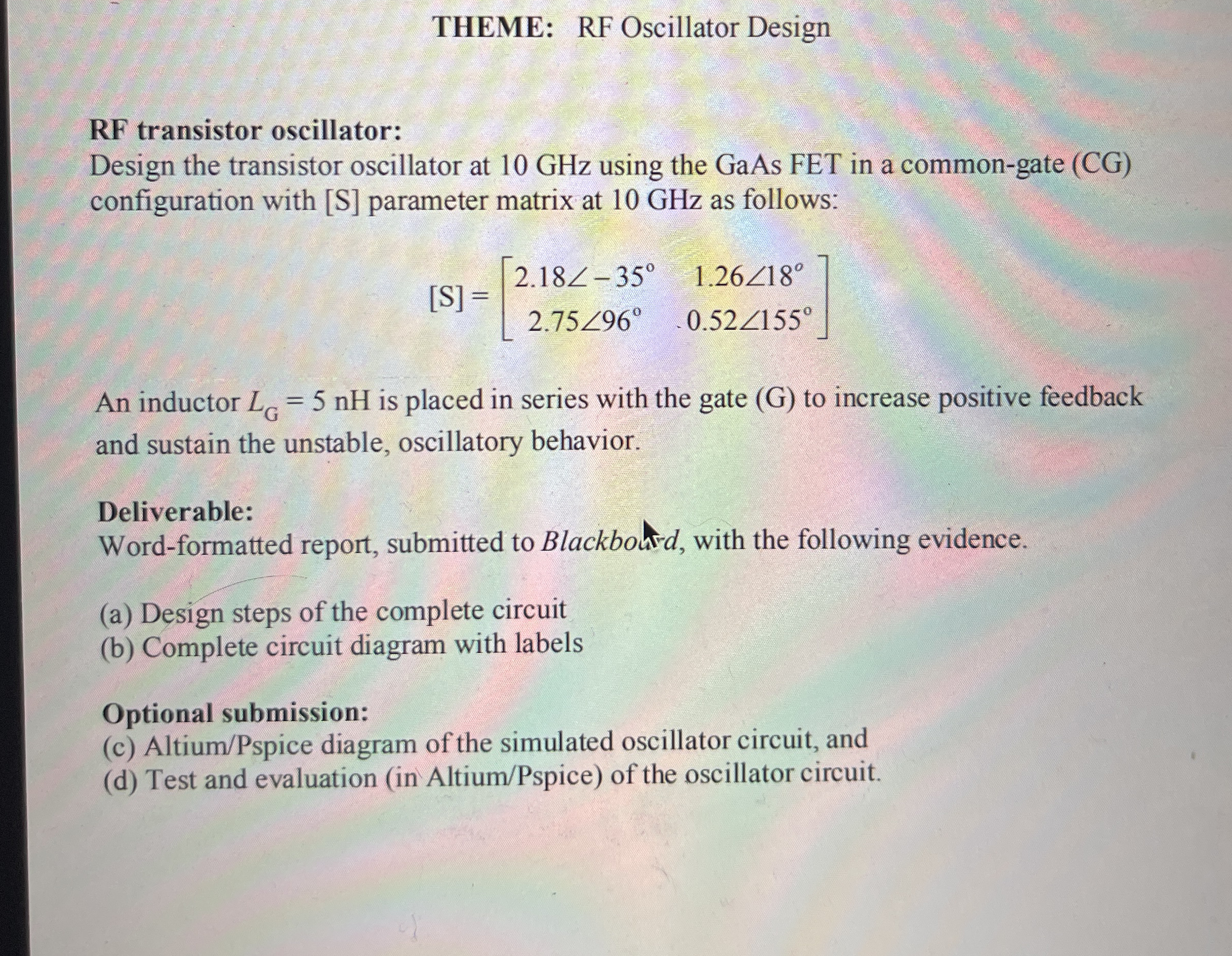
Design the transistor oscillator at GHz using the GaAs FET in a commongate CG configuration with S parameter matrix at GHz as follows:
An inductor is placed in series with the gate to increase positive feedback and sustain the unstable, oscillatory behavior.
Deliverable:
Wordformatted report, submitted to Blackboard, with the following evidence.
a Design steps of the complete circuit
b Complete circuit diagram with labels
Optional submission:
c AltiumPspice diagram of the simulated oscillator circuit, and
d Test and evaluation in AltiumPspice of the oscillator circuit.
THEME: RF Oscillator Design
RF transistor oscillator:
Design the transistor oscillator at GHz using the GaAs FET in a commongate CG configuration with S parameter matrix at GHz as follows:
An inductor is placed in series with the gate G to increase positive feedback and sustain the unstable, oscillatory behavior.
Deliverable:
Wordformatted report, submitted to Blackbohd with the following evidence.
a Design steps of the complete circuit
b Complete circuit diagram with labels
Optional submission:
c AltiumPspice diagram of the simulated oscillator circuit, and
d Test and evaluation in AltiumPspice of the oscillator circuit. Solve this question in detail, step by step,but make sure it is correct

Step by Step Solution
There are 3 Steps involved in it
1 Expert Approved Answer
Step: 1 Unlock


Question Has Been Solved by an Expert!
Get step-by-step solutions from verified subject matter experts
Step: 2 Unlock
Step: 3 Unlock


