

Question: We are building a MEMS device using a -oriented silicon substrate. The 4-inch wafer is p-type and 500 m thick. There is a 200-nm-thick PECVD
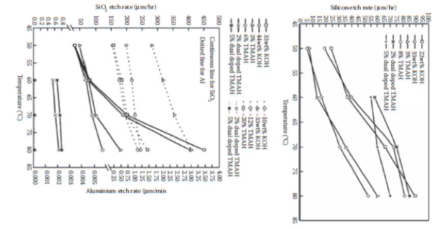
We are building a MEMS device using a -oriented silicon substrate. The 4-inch wafer is p-type and 500 m thick. There is a 200-nm-thick PECVD SiO2 thin film deposited onto the surface. We use photolithography to pattern a 750-m square onto the wafer backside, and while the photoresist is still in place, employ a 33% KOH bath at 70C to etch the device (see also the figure below). (a) What is the final size of the internal square projected onto the SiO2 on the opposite side of the wafer? (b) What would have been the minimum photolithography square feature that will etch all the way through the wafer? (c) How long will it take to etch through the SiO2 layer (see also the figure below)? (d) Once the SiO2 layer is removed, how long will it take to etch through the Si layer? (e) The etch rate of SiO2 in buffered hydrofluoric acid (BHF) is 100 nm/min. How long will it take to etch the remaining oxide layers away from the device?
Step by Step Solution
There are 3 Steps involved in it

Get step-by-step solutions from verified subject matter experts