

We saw that in a heterojunction in which the spike and notch occurred in the conduction band
Question:
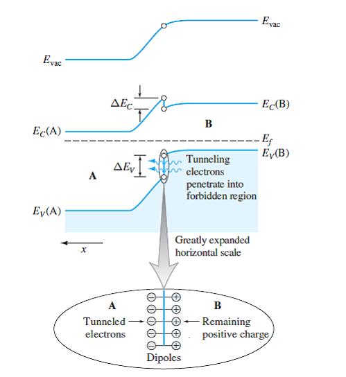
We saw that in a heterojunction in which the spike and notch occurred in the conduction band (as in Figure 6.12), it was possible for electrons in the valence band of the narrow-gap material to tunnel a short distance into the forbidden band of the wide-band-gap material. This tunneling induced a dipole that produced a discontinuity in the bands at the junction. Consider a Pn heterojunction such as that in Figure P6.3. Comment on the possibility of tunneling-induced dipoles in this case.
Figure P6.3
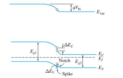
Figure 6.12 Equilibrium energy band diagram of an arbitrary Type I Np heterojunction as predicted by the electron affinity model. Electrons from the valence band of semiconductor B can tunnel a short distance into the forbidden gap of A, thus creating an interfacial dipole.
Expert Answer:
In the PN heterojunction shown in Figure P63 tunnelinginduced dipoles are not possible This is because the conduction and valence bands of the two mat... View the full answer


Stats Data and Models
ISBN: 978-0321986498
4th edition
Authors: Richard D. De Veaux, Paul D. Velleman, David E. Bock
