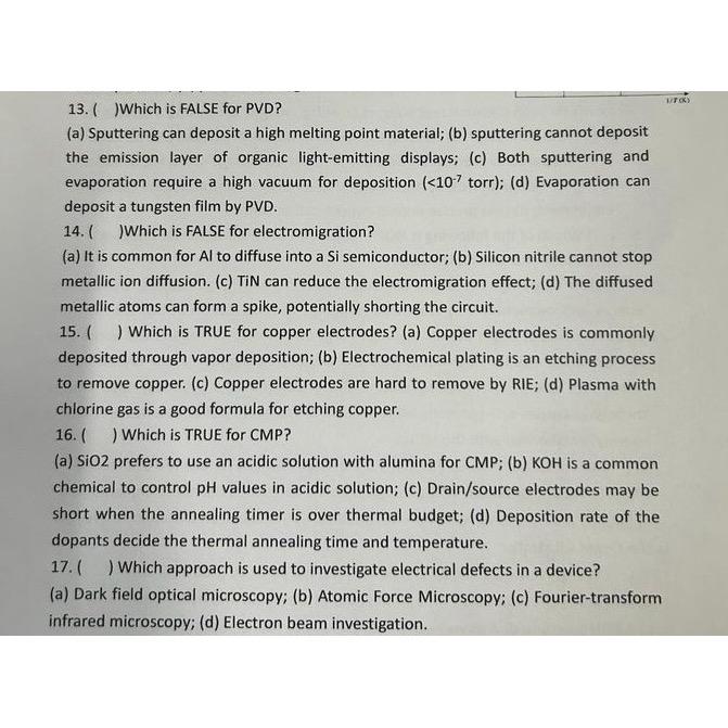
Question: ( Which is FALSE for PVD ? ( a ) Sputtering can deposit a high melting point material; ( b ) sputtering cannot deposit the
Which is FALSE for PVD
a Sputtering can deposit a high melting point material; b sputtering cannot deposit the emission layer of organic lightemitting displays; c Both sputtering and evaporation require a high vacuum for deposition torr; d Evaporation can deposit a tungsten film by PVD
Which is FALSE for electromigration?
a It is common for Al to diffuse into a Si semiconductor; b Silicon nitrile cannot stop metallic ion diffusion. c TiN can reduce the electromigration effect; d The diffused metallic atoms can form a spike, potentially shorting the circuit.
Which is TRUE for copper electrodes? a Copper electrodes is commonly deposited through vapor deposition; b Electrochemical plating is an etching process to remove copper. c Copper electrodes are hard to remove by RIE; d Plasma with chlorine gas is a good formula for etching copper.
Which is TRUE for CMP
a SiO prefers to use an acidic solution with alumina for ; b KOH is a common chemical to control values in acidic solution; c Drainsource electrodes may be short when the annealing timer is over thermal budget; d Deposition rate of the dopants decide the thermal annealing time and temperature.
Which approach is used to investigate electrical defects in a device?
a Dark field optical microscopy; b Atomic Force Microscopy; c Fouriertransform infrared microscopy; d Electron beam investigation.

Step by Step Solution
There are 3 Steps involved in it
1 Expert Approved Answer
Step: 1 Unlock


Question Has Been Solved by an Expert!
Get step-by-step solutions from verified subject matter experts
Step: 2 Unlock
Step: 3 Unlock


