

Question: Write down the VHDL behavioural description of the same D type flip flop entity and compare and contrast the two descriptions stating when one would
Write down the VHDL behavioural description of the same D type flip flop entity and compare and contrast the two descriptions stating when one would use either model with particular reference to the simulation of the D type flip flop.
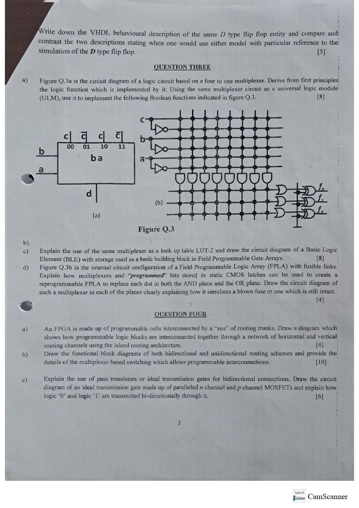
QUESTION THREE
a Figure Qa is the circuit diagram of a logic circuit based on a four to one multiplexer. Derive from first principles the logic function which is implemented by it Using the same multiplexer circuit as a universal logic module ULM use it to implement the following Boolean functions indicated in figure Q
b
c Explain the use of the same multiplexer as a look up table LUT and draw the circuit diagram of a Basic Logic Element BLE with storage used as a basic building block in Field Programmable Gate Arrays.
d Figure Qb is the internal circuit configuration of a Field Programmable Logic Array FPLA with fusible links. Explain how multiplexers and "programmed" bits stored in static CMOS latches can be used to create a reprogrammable FPLA to replace each dot in both the AND plane and the OR plane. Draw the circuit diagram of such a multiplexer in each of the planes clearly explaining how it simulates a blown fuse or one which is still intact.
QUESTION FOUR
a An FPGA is made up of programmable cells interconnected by a "sea" of routing trunks. Draw a diagram which shows how programmable logic blocks are interconnected together through a network of horizontal and vertical routing channels using the island routing architecture.
b Draw the functional block diagrams of both bidirectional and unidirectional routing schemes and provide the details of the multiplexer based switching which allows programmable interconnections.
c Explain the use of pass transistors or ideal transmission gates for bidirectional connections. Draw the circuit diagram of an ideal transmission gate made up of paralleled n channel and p channel MOSFETs and explain how. logic and logic are transmitted bidirectionally through it
Sraredith
OGCanscana
CamScanner
Step by Step Solution
There are 3 Steps involved in it
1 Expert Approved Answer
Step: 1 Unlock

Question Has Been Solved by an Expert!
Get step-by-step solutions from verified subject matter experts
Step: 2 Unlock
Step: 3 Unlock