

Question: you are required to write the program using C programming language* ON ATMEL STUDIO . You must use at least one interrupt switch for any
you are required to write the program using C programming language* ON ATMEL STUDIO . You must use at least one interrupt switch for any given tasks, and Timer0 to perform delay ON ATMEGA32A
- You may design referring to the schematic in Figure 1. Figure 1 is just an example. You can always modify the peripherals interfacing that suit your design requirements.
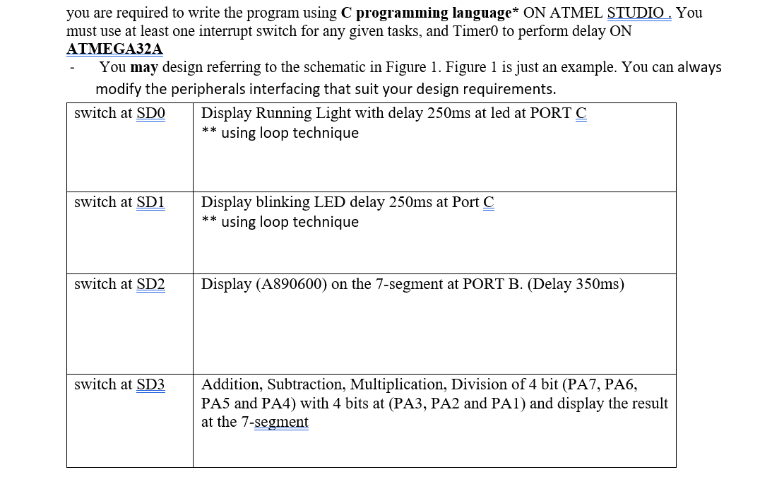
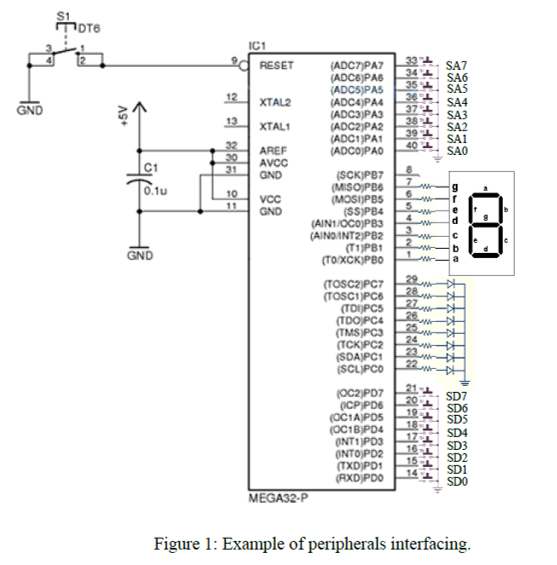
you are required to write the program using C programming language* ON ATMEL STUDIO . You must use at least one interrupt switch for any given tasks, and Timero to perform delay ON ATMEGA32A You may design referring to the schematic in Figure 1. Figure 1 is just an example. You can always modify the peripherals interfacing that suit your design requirements. switch at SDO Display Running Light with delay 250ms at led at PORT C using loop technique *** switch at SD1 Display blinking LED delay 250ms at Port C using loop technique *** switch at SD2 Display (A890600) on the 7-segment at PORT B. (Delay 350ms) switch at SD3 Addition, Subtraction, Multiplication, Division of 4 bit (PA7, PA6, PA5 and PA4) with 4 bits at (PA3, PA2 and PAI) and display the result at the 7-segment IC1 331 GND +5V SA7 3411 SA6 35+ SAS 361 SA4 371 SA3 38 SA2 391 SA1 40 SAO C1 0.10 g r d 5 ww 4 3 2 W GND RESET (ADC7)PAZ (ADC6PAS (ADC5)PAS 12 XTAL2 (ADC4)PA4 (ADC3PA3 13 XTAL1 (ADC2)PA2 (ADC1)PA1 32 AREF (ADCOPAO 30 AVOC 31 GND (SCKPB7 (MISOPB6 10 VCC (MOSI)PBS 11 GND (SSPB4 (AIN1IOCOPB3 (AINO INT2PB2 (T1)PB1 (TOIXCK PBO (TOSC2)PC7 (TOSCIPCB (TDI)PCS (TDO]PC4 (TMS)PC3 (TCKPC2 (SDA)PCI (SCLIPCO (OC2P07 (CPPD6 (OCTA PDS (OC1B)PD4 (INT1)PD3 (INTO)PD2 (TXD PD1 (AXD)PDO MEGA32.P 28 22 DH 2. H DH 25 24 2a 22 21 20 121 SD7 SD6 SDS SD4 1701 14 SDO Figure 1: Example of peripherals interfacing. you are required to write the program using C programming language* ON ATMEL STUDIO . You must use at least one interrupt switch for any given tasks, and Timero to perform delay ON ATMEGA32A You may design referring to the schematic in Figure 1. Figure 1 is just an example. You can always modify the peripherals interfacing that suit your design requirements. switch at SDO Display Running Light with delay 250ms at led at PORT C using loop technique *** switch at SD1 Display blinking LED delay 250ms at Port C using loop technique *** switch at SD2 Display (A890600) on the 7-segment at PORT B. (Delay 350ms) switch at SD3 Addition, Subtraction, Multiplication, Division of 4 bit (PA7, PA6, PA5 and PA4) with 4 bits at (PA3, PA2 and PAI) and display the result at the 7-segment IC1 331 GND +5V SA7 3411 SA6 35+ SAS 361 SA4 371 SA3 38 SA2 391 SA1 40 SAO C1 0.10 g r d 5 ww 4 3 2 W GND RESET (ADC7)PAZ (ADC6PAS (ADC5)PAS 12 XTAL2 (ADC4)PA4 (ADC3PA3 13 XTAL1 (ADC2)PA2 (ADC1)PA1 32 AREF (ADCOPAO 30 AVOC 31 GND (SCKPB7 (MISOPB6 10 VCC (MOSI)PBS 11 GND (SSPB4 (AIN1IOCOPB3 (AINO INT2PB2 (T1)PB1 (TOIXCK PBO (TOSC2)PC7 (TOSCIPCB (TDI)PCS (TDO]PC4 (TMS)PC3 (TCKPC2 (SDA)PCI (SCLIPCO (OC2P07 (CPPD6 (OCTA PDS (OC1B)PD4 (INT1)PD3 (INTO)PD2 (TXD PD1 (AXD)PDO MEGA32.P 28 22 DH 2. H DH 25 24 2a 22 21 20 121 SD7 SD6 SDS SD4 1701 14 SDO Figure 1: Example of peripherals interfacing
Step by Step Solution
There are 3 Steps involved in it

Get step-by-step solutions from verified subject matter experts