

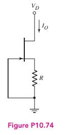
A JFET circuit is biased with the current source in Figure P10.74. The transistor parameters are: (I_{D
Question:
A JFET circuit is biased with the current source in Figure P10.74. The transistor parameters are: \(I_{D S S}=4 \mathrm{~mA}, V_{P}=-4 \mathrm{~V}\), and \(\lambda=0\). Design the circuit such that \(I_{O}=2 \mathrm{~mA}\). What is the minimum value of \(V_{D}\) such that the transistor is biased in the saturation region?
Fantastic news! We've Found the answer you've been seeking!
Step by Step Answer:

Answered By
PALASH JHANWAR
I am a Chartered Accountant with AIR 45 in CA - IPCC. I am a Merit Holder ( B.Com ). The following is my educational details.
PLEASE ACCESS MY RESUME FROM THE FOLLOWING LINK: https://drive.google.com/file/d/1hYR1uch-ff6MRC_cDB07K6VqY9kQ3SFL/view?usp=sharing
3+ Reviews
10+ Question Solved
Related Book For 

Microelectronics Circuit Analysis And Design
ISBN: 9780071289474
4th Edition
Authors: Donald A. Neamen
Question Posted:
