

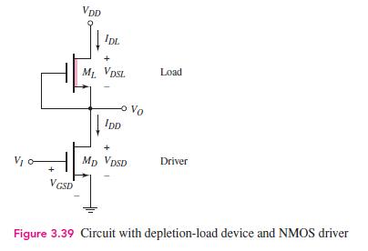
Consider the circuit in Figure 3.39 with a depletion load. Assume the circuit is biased at (V_{D
Question:
Consider the circuit in Figure 3.39 with a depletion load. Assume the circuit is biased at \(V_{D D}=3.3 \mathrm{~V}\), and assume transistor threshold voltages of \(V_{T N D}=0.4 \mathrm{~V}\) and \(V_{T N L}=-0.75 \mathrm{~V}\). Also assume \(k_{n}^{\prime}=80 \mu \mathrm{A} / \mathrm{V}^{2}\). Design the circuit such that \(V_{O}=0.05 \mathrm{~V}\) when \(V_{I}=3.3 \mathrm{~V}\) and that the maximum power dissipation is \(150 \mu \mathrm{W}\).
Figure 3.39:-
Fantastic news! We've Found the answer you've been seeking!
Step by Step Answer:

Answered By
Lamya S
Highly creative, resourceful and dedicated High School Teacher with a good fluency in English (IELTS- 7.5 band scorer) and an excellent record of successful classroom presentations.
I have more than 2 years experience in tutoring students especially by using my note making strategies.
Especially adept at teaching methods of business functions and management through a positive, and flexible teaching style with the willingness to work beyond the call of duty.
Committed to ongoing professional development and spreading the knowledge within myself to the blooming ones to make them fly with a colorful wing of future.
I do always believe that more than being a teacher who teaches students subjects,...i rather want to be a teacher who wants to teach students how to love learning..
Subjects i handle :
Business studies
Management studies
Operations Management
Organisational Behaviour
Change Management
Research Methodology
Strategy Management
Economics
Human Resource Management
Performance Management
Training
International Business
Business Ethics
Business Communication
Things you can expect from me :
- A clear cut answer
- A detailed conceptual way of explanation
- Simplified answer form of complex topics
- Diagrams and examples filled answers
46+ Reviews
54+ Question Solved
Related Book For 

Microelectronics Circuit Analysis And Design
ISBN: 9780071289474
4th Edition
Authors: Donald A. Neamen
Question Posted:
