

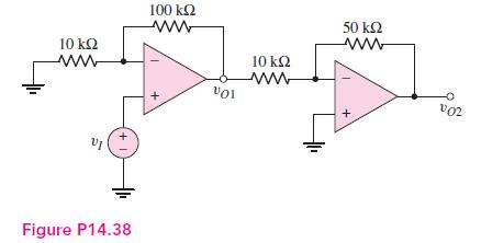
For each op-amp in the circuit in Figure P14.38, the offset voltage is (V_{O S}=10 mathrm{mV}) and
Question:
For each op-amp in the circuit in Figure P14.38, the offset voltage is \(V_{O S}=10 \mathrm{mV}\) and the input bias currents are \(I_{B 1}=I_{B 2}=2 \mu \mathrm{A}\).
(a) Find the worst-case output voltages \(v_{O 1}\) and \(v_{O 2}\) for \(v_{I}=0\).
(b) Design compensation circuits to adjust both \(v_{O 1}\) and \(v_{O 2}\) to zero when \(v_{I}=0\).
Fantastic news! We've Found the answer you've been seeking!
Step by Step Answer:

Answered By
Mugdha Sisodiya
My self Mugdha Sisodiya from Chhattisgarh India. I have completed my Bachelors degree in 2015 and My Master in Commerce degree in 2016. I am having expertise in Management, Cost and Finance Accounts. Further I have completed my Chartered Accountant and working as a Professional.
Since 2012 I am providing home tutions.
2+ Reviews
10+ Question Solved
Related Book For 

Microelectronics Circuit Analysis And Design
ISBN: 9780071289474
4th Edition
Authors: Donald A. Neamen
Question Posted:
