

Question: In a particular application, it is necessary to implement the block diagram shown in Figure 454. The maximum individual OP AMP gain cannot exceed 2000.
In a particular application, it is necessary to implement the block diagram shown in Figure 4–54. The maximum individual OP AMP gain cannot exceed 2000. The input resistance of the first signal stage must be at least 10 kΩ. The nominal input signal υ1 is 1 μV.
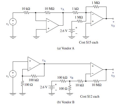
Two vendors have provided competitive solutions, shown in Figure 4–55. Choose the best solution based on achieving the desired output considering: cost, parts count, variety of parts needed, and power usage
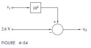
2.6 Vo FIGURE 4-54 106 + Vo
Step by Step Solution
There are 3 Steps involved in it
1 Expert Approved Answer
Step: 1 Unlock

Question Has Been Solved by an Expert!
Get step-by-step solutions from verified subject matter experts
Step: 2 Unlock
Step: 3 Unlock