

Question: Using the instrumentation amplifier shown in Figure 4=78 ( Example 4-27), design a circuit that will produce the output (v_{mathrm{O}}=5 times 10^{5}left(v_{1}-v_{2}ight)). No single OP
Using the instrumentation amplifier shown in Figure 4=78 ( Example 4-27), design a circuit that will produce the output \(v_{\mathrm{O}}=5 \times 10^{5}\left(v_{1}-v_{2}ight)\). No single OP AMP can have a gain greater than 5000 .
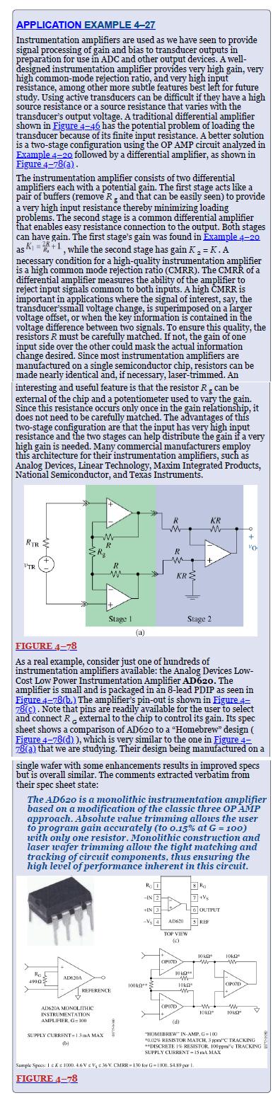
APPLICATION EXAMPLE 4-27 Instrumentation amplifiers are used as we have seen to provide signal processing of gain and bias to transducer outputs in preparation for use in ADC and other output devices. A well- designed instrumentation amplifier provides very high gain, very high common-mode rejection ratio, and very high input resistance, among other more subtle features best left for future study. Using active transducers can be difficult if they have a high source resistance or a source resistance that varies with the transducer's output voltage. A traditional differential amplifier shown in Figure 4-46 has the potential problem of loading the transducer because of its finite input resistance. A better solution is a two-stage configuration using the OP AMP circuit analyzed in Example 4-20 followed by a differential amplifier, as shown in Figure 4-78(a). The instrumentation amplifier consists of two differential amplifiers each with a potential gain. The first stage acts like a pair of buffers (remove R, and that can be easily seen) to provide a very high input resistance thereby minimizing loading problems. The second stage is a common differential amplifier that enables easy resistance connection to the output. Both stages can have gain. The first stage's gain was found in Example 4-20 as K+1, while the second stage has gain K = K.A 3 necessary condition for a high-quality instrumentation amplifier is a high common mode rejection ratio (CMRR). The CMRR of a differential amplifier measures the ability of the amplifier to reject input signals common to both inputs. A high CMRR is important in applications where the signal of interest, say, the transducer'ssmall voltage change, is superimposed on a larger voltage offset, or when the key information is contained in the voltage difference between two signals. To ensure this quality, the resistors R must be carefully matched. If not, the gain of one input side over the other could mask the actual information change desired. Since most instrumentation amplifiers are manufactured on a single semiconductor chip, resistors can be made nearly identical and, if necessary, laser-trimmed. An interesting and useful feature is that the resistor Rg can be external of the chip and a potentiometer used to vary the gain. Since this resistance occurs only once in the gain relationship, it does not need to be carefully matched. The advantages of this two-stage configuration are that the input has very high input resistance and the two stages can help distribute the gain if a very high gain is needed. Many commercial manufacturers employ this architecture for their instrumentation amplifiers, such as Analog Devices, Linear Technology, Maxim Integrated Products, National Semiconductor, and Texas Instruments. RTR TR Re 4990 AD0204 M R AD620A MONOLITHIC R m INSTRUMENTATION AMPLIFIER, G-100 Stage 1 (a) REFERENCE SUPPLY CURRENT=13mA MAX (b) FIGURE 4-78 As a real example, consider just one of hundreds of instrumentation amplifiers available: the Analog Devices Low- Cost Low Power Instrumentation Amplifier AD620. The amplifier is small and is packaged in an 8-lead PDIP as seen in Figure 4-78(b) The amplifier's pin-out is shown in Figure 4- 78(c). Note that pins are readily available for the user to select and connect R external to the chip to control its gain. Its spec sheet shows a comparison of AD620 to a "Homebrew" design ( Figure 4-78(d)), which is very similar to the one in Figure 4- 78(a) that we are studying. Their design being manufactured on a single wafer with some enhancements results in improved specs but is overall similar. The comments extracted verbatim from their spec sheet state: R m The AD620 is a monolithic instrumentation amplifier based on a modification of the classic three OP AMP approach. Absolute value trimming allows the user to program gain accurately (to 0.15% at G = 100) with only one resistor. Monolithic construction and laser wafer trimming allow the tight matching and tracking of circuit components, thus ensuring the high level of performance inherent in this circuit. 1002 KR Ra IN 2 +INE -Vs 4 AD620 TOP VIEW (c) OPOZD 102 ww 10KG W OP07D Stage 2 (d) KR + Ra Sample Spees: 1 ks 1000 46V V36V. CMRR-130 for G-100, $4.89 per l FIGURE 4-78 6 OUTPUT 5 REF 10 ka 10k www. -w W JORD "O OPOZD ww 10RC "HOMEBR MATCH 300C TRACKING "HOMEBREW" IN-AMP, G-100 02% RESISTOR **DISCRETE 1% RESISTOR, 100ppm TRACKING SUPPLY CURRENT-15 mA MAX
Step by Step Solution
3.36 Rating (149 Votes )
There are 3 Steps involved in it
The instrumentation amplifier has two stages with gains of K 2RR ... View full answer

Get step-by-step solutions from verified subject matter experts