

In chemical vapor deposition (CVD), a semiconducting or insulating solid material is formed in a reaction between
Question:
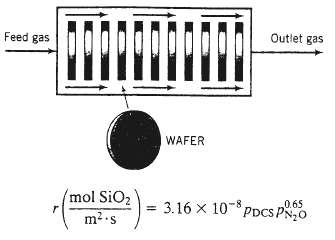
In chemical vapor deposition (CVD), a semiconducting or insulating solid material is formed in a reaction between a gaseous species and a species adsorbed on the surface of silicon wafers (disks about 10 cm in diameter and 1 mm thick). The coated wafers are subjected to further processing to produce the microelectronic chips in computers and most other electronic devices in use today. In one such process, silicon dioxide (MW = 60.06, SO = 2.67) is formed in the reaction between gaseous dichiorosilane (DCS) and adsorbed nitrous oxide: SiH2Cl2?(g) + 2N2O (ads) SiO2(s) + 2N2 (g) + 2 HC1 (g) A mixture of DCS and N20 flows through a ?boat reactor??a horizontal pipe in which 50?100 silicon wafers about 12 cm in diameter and 1 mm thick are set upright along the reactor length, with about 20 mm separation between each wafer. A side view of the reactor is shown below: The feed gas enters the reactor at a rate of 3.74 SCMM (standard cubic meters per minute) and contains 22.0 mole% DCS and the balance N2O. In the reactor, the gas flows around the wafers, DCS and N2O diffuse into the spaces between the wafers, N2O is adsorbed on the wafer surfaces, and the adsorbed N2O reacts with gaseous DCS. The silicon dioxide formed remains on the surface, and the nitrogen and hydrogen chloride go into the gas phase and eventually leave the reactor with the unconsumed reactants. The temperature and absolute pressure in the reactor are constant at 900?C and 604millitorr.
(a) The percentage conversion of DCS at a certain axial position (distance along the length of the reactor) is 60%. Calculate the volumetric flow rate (m3/min) of gas at this axial position.
(b) The rate of deposition of silicon dioxide per unit area of wafer surface is given by the formula where PDCS?and PN2O are the partial pressures of DCS and N2O in millitorr. What is r at the axial position in the reactor where the DCS conversion is 60%?
(c) Consider a wafer located at the axial position determined in part (b). How thick is the silicon dioxide layer on that wafer after two hours of reactor operation, assuming that gas diffusion is rapid enough at the low reactor pressure for the composition of the gas (and hence the component partial pressures) to be uniform over the wafer surface? Express your answer in angstroms where 1 A = 1.0 x 10⁻¹⁰ m would the thickness be greater or less than this value at an axial position closer to the reactor entrance? Briefly explain your answer.
Step by Step Answer:
374 SCMM n molmin 0220 DCS 0780 N0 V mmin 900C 604 mtorr 60 DCS conversion n mol DCS min n mol NOmin ...View the full answer


Elementary Principles of Chemical Processes
ISBN: 978-0471720638
3rd Edition
Authors: Richard M. Felder, Ronald W. Rousseau
