

Question: Determine the required bias current and device sizes to design a source-coupled pair to have the following two characteristics. First, the small-signal transconductance with zero
Determine the required bias current and device sizes to design a source-coupled pair to have the following two characteristics. First, the small-signal transconductance with zero differential input voltage should be 1.0 mA/V. Second, a differential input voltage of 0.2 V should result in a differential output current of 85 percent of the maximum value. Assume that the devices are n-channel transistors that are made with the technology summarized in Table 2.4. Use a drawn device channel length of 1µm. Neglect channel-length modulation, and assume Xd= 0.
Table 2.4:
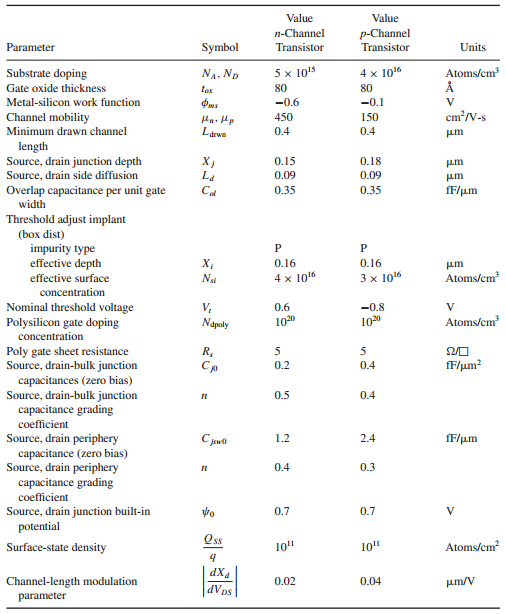
Value Value p-Channel n-Channel Units Parameter Symbol Transistor Transistor 5 x 10⁵ 4 x 10⁶ Substrate doping Atoms/cm NA, Np Gate oxide thickness 80 80 lox Metal-silicon work function -0.6 -0.1 cm/V-s Channel mobility Minimum drawn channel 450 150 Lrwn 0.4 0.4 um length Source, drain junction depth Source, drain side diffusion Overlap capacitance per unit gate width Threshold adjust implant (b dist) impurity type effective depth effective surface 0.15 0.18 um La 0.09 0.09 um 0.35 0.35 fF/um , Nsi 0.16 0.16 um Atoms/cm 3 x 10¹⁶ 4 x 10¹⁶ concentration Nominal threshold voltage Polysilicon gate doping concentration Poly gate sheet resistance Source, drain-bulk junction capacitances (zero bias) Source, drain-bulk junction capacitance grading V, Napoly 0.6 1020 -0.8 Atoms/cm? 1020 R, Cp fF/um? 0.2 0.4 0.5 0.4 coefficient Source, drain periphery capacitance (zero bias) Source, drain periphery capacitance grading fF/um 1.2 2.4 0.4 0.3 coefficient Source, drain junction built-in potential 0.7 0.7 Oss Surface-state density 10" 10" Atoms/cm PXP dV ps Channel-length modulation 0.02 0.04 um/V parameter
Step by Step Solution
3.59 Rating (156 Votes )
There are 3 Steps involved in it
From Table 24 194 AV 2 K I d 085 I tail Also Substit... View full answer

Get step-by-step solutions from verified subject matter experts
Document Format (2 attachments)
1528_605d88e1ac0aa_686808.pdf
180 KBs PDF File
1528_605d88e1ac0aa_686808.docx
120 KBs Word File