

Question: For the folded-active-cascode op amp in Fig. 6.30, choose the device sizes to give a peak-peak output swing of at least 2.5 V. Use the
For the folded-active-cascode op amp in Fig. 6.30, choose the device sizes to give a peak-peak output swing of at least 2.5 V. Use the 0.4 μm CMOS model parameters in Table 2.4 except let γ = 0.25 V½and Xd= 0 for all transistors and Vt0= 0.7 V and ˆ’0.7 V for n-channel and p-channel transistors, respectively. Assume the drawn channel length is L = 1μm is used for all transistors to simplify the design. With IBIAS= 25 μA, the bias currents should be |ID5| = ID11ID12 = ID25= |ID35|=200 μA. Assume VDD = VSS=1.65 V and that the matching is perfect. When the dc input voltage VI=0, assume that all transistors except M106and M114operate in the active region with equal overdrive magnitudes. To make the gain insensitive to small shifts in the operating point, design the circuit so that the magnitude of the drain-source voltage for each transistor operating in the active region exceeds the magnitude of its over-drive by at least 100 mV. Ignore the body effect in the hand calculations. Use SPICE to verify your design, to choose the widths of M106and M114, and to deter-mine the gain. Also, use SPICE to determine the gain if Vt0= 0.6V for n-channel transistors andVt0= ˆ’0.8 V for p-channel transistors, as given in Table 2.4. Explain the resulting change in the op-amp again.
Figure 6.30
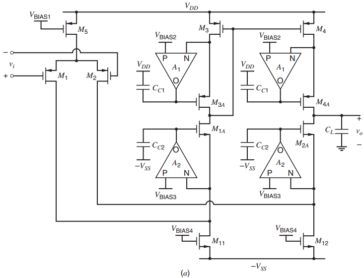
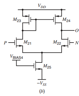
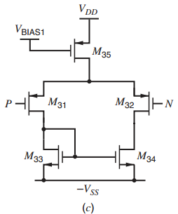
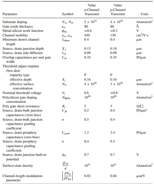
Table 2.4
VDD M4 VBIAS1 M VBIAS2 M5 VBIAS2 N, A1 P VDp VDD A1 I. M2 M1 Cc1 MAA M1A 2 Cc2 Cc2 A2 -Vss A2 -Vss VBIAS3 VBIAS3 VBIAS4 VBIAS4 M12 M11 -Vss (a) VDD M24 M23 M21 M22 EN P BIASA M25 -Vss ()
Step by Step Solution
3.47 Rating (163 Votes )
There are 3 Steps involved in it
M 4 M 4A M 2A and M 12 should all operate in the active region for a peak to peak output swing of 25 ... View full answer

Get step-by-step solutions from verified subject matter experts