

Question: For this problem, use the op amp in Fig. 12.23 and the CMFB scheme in Fig. 12.17. Use the complement of the amplifier in Fig.
For this problem, use the op amp in Fig. 12.23 and the CMFB scheme in Fig. 12.17. Use the complement of the amplifier in Fig. 12.16b as the CM-sense amplifier, modified to give a negative dc gain. Assume the source followers in Fig. 12.17 have a low-frequency gain of 0.95 and Rcs= 15 kΩ. Use the transistor and op-amp operating-point data given in the example in Section 12.6.1.
Fig. 12.23:
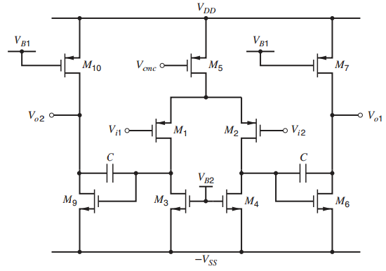
Fig. 12.16(b)
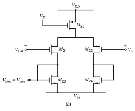
Figure 12.17:
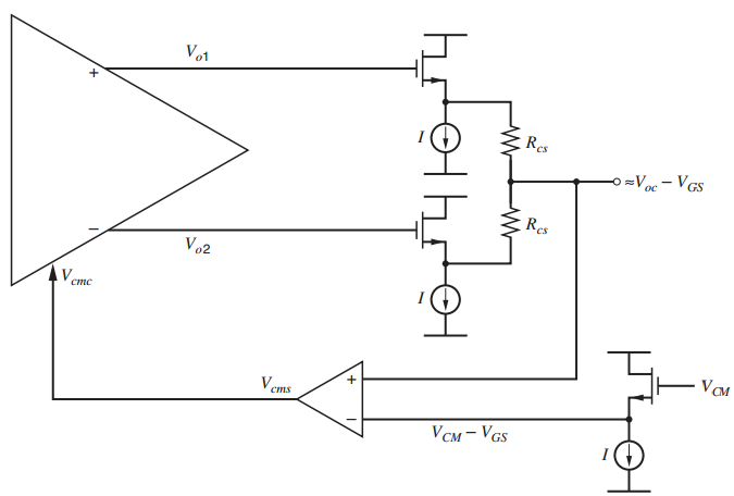
(a) Design the CM-sense amplifier so that the total low-frequency gain acms0 = voc / vcms = ˆ’0.71, which is the same value as in the example in Section 12.6.1.
(b) With this CMFB circuit, what are the swing limits for each op-amp output voltage (Vo1 and Vo2)? Assume that the biasing current source in each source follower in Fig. 12.17 is implemented with a NMOS transistor, and the current-source and source-follower transistors operate with VGS = 0.8 V and Vov = 0.2V. For simplicity, assume VGS is constant and take γ = 0.
(c) What value of VCM gives the largest symmetric output swing?
(d) Verify that this CMFB circuit works correctly by running a SPICE simulation. Use the value of VCM from part (c).
VDD V1 V 1 M5 V one M10 Vo1 o Vi2 M2 Vo2 M1 Vit V2 M6 Mg -Vss VDD VB M25 oV. M21 M22 VCM M24 M23 Veme = Vems -Vss (b)
Step by Step Solution
3.40 Rating (163 Votes )
There are 3 Steps involved in it
a 071 Choose M23 to Match M5 WL 23 WL 5 25 Choose M25 to have an overdrive of 02 V I D25 ... View full answer

Get step-by-step solutions from verified subject matter experts
Document Format (2 attachments)
1528_605d88e1c0476_687011.pdf
180 KBs PDF File
1528_605d88e1c0476_687011.docx
120 KBs Word File