New Semester
Started
Get
50% OFF
Study Help!
--h --m --s
Claim Now
Question Answers
Textbooks
Find textbooks, questions and answers
Oops, something went wrong!
Change your search query and then try again
S
Books
FREE
Study Help
Expert Questions
Accounting
General Management
Mathematics
Finance
Organizational Behaviour
Law
Physics
Operating System
Management Leadership
Sociology
Programming
Marketing
Database
Computer Network
Economics
Textbooks Solutions
Accounting
Managerial Accounting
Management Leadership
Cost Accounting
Statistics
Business Law
Corporate Finance
Finance
Economics
Auditing
Tutors
Online Tutors
Find a Tutor
Hire a Tutor
Become a Tutor
AI Tutor
AI Study Planner
NEW
Sell Books
Search
Search
Sign In
Register
study help
business
principles algorithms and systems
Computer Systems 5th Edition J Stanley Warford - Solutions
28. Implement a new nonunary instruction in place of NOP called MULA that multiplies the operand by the accumulator and puts the result in the accumulator. Allow only direct addressing. Use the interative shift-and-add algorithm of Problem 6.24. NZC should should correlate with the new value in the
29. Direct addressing is immediate addressing deferred. Indirect addressing is direct addressing deferred. You can carry this concept one level further with double indirect addressing, which is indirect addressing deferred. Implement a new instruction in place of NOP0 with mnemonic STWADI, which
30. Implement a new nonunary instruction in place of NOP called BOOLO, which means Boolean output. It should output false if the operand is zero and true otherwise. Allow immediate, direct, and stack-relative addressing. None of the status flags are affected. Use the test program provided in the
31. Implement a new unary instruction in place of NOP0 called STKADD. It should replace the two topmost items on the stack with their sum. Set NZVC according to the results of the addition.Use the test program provided in the Pep/9 app to test the features of the new instruction.
32. Implement a new nonunary instruction in place of NOP called XORA, which computes the bitwise exclusive OR operation with the operand and the accumulator, placing the result in the accumulator. Allow only direct addressing. Status bits NZ should be set according to the results of the operation,
33. This problem is to implement new nonunary instructions to process floating point numbers.Assume that floating point numbers are stored with all the special values of IEEE 754 but with a two-byte cell having one sign bit, six exponent bits, nine significand bits, and a hidden bit. The exponent
1. Using the format of Figure 9.4, devise a job execution sequence for which the first-fit algorithm would require compaction before the best-fit algorithm. Sketch the fragmentation in main memory just before compaction is required for each algorithm.
2. Figure 9.10 shows how a page table in a paging system performs the same transformation of the logical address as the base register does in a multiprogramming system. The equivalent job of the bound register is not shown in the figure. *(a) To protect other processes’ memory space from
3. Suppose the page size in a paging system is 512 bytes. (a) If most of the files are large—that is, much greater than 512 bytes—what do you suppose is the average internal fragmentation(in bytes of unused space) for each file? Explain your reasoning. (b) How would your answer to part (a)
4. A computer has 12-bit addresses and a main memory that is divided into 16 frames. Memory management uses demand paging. *(a) How many bytes is virtual memory? (b) How many bytes are in each page? (c) How many bits are in the offset of a logical and physical address? (d) What is the maximum
5. Answer Exercise 4 for a computer with n-bit addresses and a memory divided into 2k frames.
6. For which pages in Figure 9.12 is the image on disk an exact replica of the page in main memory?
7. Verify the data of Figure 9.15(b), which shows Bélády’s anomaly, for the sequence of page references given in the text. Display the content of the frames in the format of Figure 9.13.
8. Devise a sequence of 12 page references for which the FIFO page-replacement algorithm is better than the LRU algorithm.
9. Plot the graph of Figure 9.15(b) for the page reference sequence in Figure 9.13 using the FIFO page-replacement algorithm. On the same graph, plot the data for the LRU algorithm.
10. If the operating system could predict the future, it could select the replacement page such that the next page fault is delayed as long as possible. Such an algorithm is called OPT, the optimum page-replacement algorithm. It is a useful theoretical algorithm because it represents the best you
11. Suppose a disk rotates at 5,400 revolutions per minute and has each surface divided into 16 sectors. *(a) What is the maximum possible latency time? Under what circumstance will that occur? (b) What is the minimum possible latency time? Under what circumstance will that occur? (c) From (a) and
12. (a) How many data bits are required to store one of the decimal digits 0 through 9? *(b)How many parity bits are required to detect a single error? (c) Write a single-error detection code using even parity. Underline the parity bits. (d) What is the code distance of your code?
13. (a) What must the code distance be to detect five errors? (b) What must the code distance be to correct five errors?
14. (a) Which entries in Figure 9.24 represent perfect codes? (b) Augment the table in Figure 9.24 with additional entries to include all the perfect codes between m = 4 and m = 128. Be sure to include the overhead value. (c) What can you conclude about the cost of restricting the number of data
15. (a) How many data bits are required to store one of the decimal digits 0 through 9? (b) How many parity bits are required to correct a single error? (c) Write a single-error correction code using even parity. Underline the parity bits. (d) What is the code distance of your code?
16. A set of eight data bits is transmitted with the single-error correction code of Figure 9.25.For each of the received bit patterns below, state whether an error occured. If it did, correct the error.(a) 1 0 0 1 1 0 1 0 1 0 0 1(b) 1 1 0 1 0 0 1 1 0 0 1 0(c) 0 0 0 0 1 0 1 1 0 1 0 0(d) 1 0 1 1 0 0
17. Figure 9.28 shows a RAID system with eight physical disks. (a) With six physical disks, how many mirror controllers and stripe controllers would you need for level 01 and for level 10?(b) With 2n disks in general (so that n = 4 in Figure 9.28), how many mirror controllers and stripe controllers
18. (a) Figure 9.28 shows the RAID level 01 and RAID level 10 systems with eight physical disks. Draw the equivalent systems for level 01 and level 10 with four physical disks. (b)Assume that two disks go bad. The sequence BBGG means that the first and second disks are bad and the third and fourth
19. You have a RAID level 4 system with eight data disks and one parity disk. (a) How many disk reads and disk writes must you make to write one data stripe if you do not make use of the old data and parity values? (b) How many disk reads and disk writes must you make to write one data stripe if
1. (a) Prove the zero theorem x + 1 = 1 with Boolean algebra. Give a reason for each step in your proof. Hint: Expand the 1 on the left with the complement property and then use the idempotent property. (b) Show the dual proof of part (a).
2. (a) Prove with Boolean algebra the absorption property, x + x · y = x. Give a reason for each step in your proof. (b) Show the dual proof of part (a).
3. (a) Prove with Boolean algebra the consensus theorem x · y + x′ · z + y · z = x · y + x′· z.Give a reason for each step in your proof. (b) Show the dual proof of part (a).
4. Prove De Morgan’s law, (a + b)′ = a′· b′, by giving the dual of the proof in the text. Give a reason for each step in your proof.
5. (a) Prove the general form of De Morgan’s law,(a1 · a2 · · · · · an)′ = a1′ + a2′ + · · · + an′ where n ≥ 2 from De Morgan’s law for two variables using mathematical induction. (b) Show the dual proof of part (a).
6. (a) Prove with Boolean algebra that (x + y) · (x′ + y) = y. Give a reason for each step in your proof. (b) Show the dual proof of part (a).
7. (a) Prove with Boolean algebra that (x + y) + (y · x′) = x + y. Give a reason for each step in your proof. (b) Show the dual proof of part (a).
8. *(a) Draw a three-input OR gate, its Boolean expression, and its truth table, as in Figure 10.10. (b) Do part (a) for the three-input NAND gate. (c) Do part (a) for the three-input NOR gate.
9. For each of the following Boolean properties or theorems, state the set theory interpretation:*(a) x + 0 = x(b) x · 1 = x(c) x + x′ = 1(d) x · x′ = 0(e) x · x = x(f) x + x = x(g) x · 0 = 0
10. (a) Show the associative property for the OR operation using Venn diagrams with x, y, and z overlapping regions. Sketch the following regions to show that region (3) is the same as region (6):(1) (x + y)(2) z(3) (x + y) + z(4) x(5) (y + z)(6) x + (y + z)(b) Do the dual of part (a).
11. (a) Show the distributive property using Venn diagrams with x, y, and z overlapping regions.Sketch the following regions to show that region (3) is the same as region (6):(1) x(2) y · z(3) x + y · z(4) (x + y)(5) (x + z)(6) (x + y) · (x + z)(b) Do the dual of part (a).
12. (a) Show De Morgan’s law using Venn diagrams with a and b overlapping regions. Sketch the following regions to show that region (2) is the same as region (5):(1) a · b(2) (a · b)′(3) a′(4) b′(5) a′ + b′(b) Do the dual of part (a).
13. Although a Boolean variable for a combinational circuit can have only two values, 1 or 0, Boolean algebra can describe a system where a variable can have one of four possible values—0, 1, A, or B. Such a system corresponds to the description of subsets of {a, b}where 1 = {a, b} (the universal
14. The exclusive NOR gate, written XNOR, is equivalent to an XOR followed by an inverter. *(a) Draw the symbol for a two-input XNOR gate. (b) Construct its truth table. (c) The XNOR is also called a comparator. Why?
15. Draw the nonabbreviated logic diagram for the following Boolean expressions. You may use XOR gates.*(a) ((a′)′)′*(b) (((a′)′)′)′(c) a′b + ab′(d) ab + a′b′(e) ab + ab′ + a′b (f) ((ab ⊕ b′)′ + a′b)′(g) (a′bc + a)b (h) (ab′c)′(ac)′(i) ((ab)′(b′c)′
16. Draw the abbreviated logic diagram for the Boolean expressions of Exercise 15. You may use XOR gates.
17. Construct the truth tables for the Boolean expressions of Exercise 15.
18. Write the Boolean expressions for the logic diagrams of FIGURE 10.63 . FIGURE 10.63 The logic diagrams for Exercise 18. b 300 (a) a (c) (b)
19. Write the Boolean AND-OR expression for the following:*(a) function y in Figure 10.3(b) function y in Figure 10.4(c) function x in Figure 10.17(d) the NAND gate in Figure 10.7(a)(e) the XOR gate in Figure 10.7(c)
20. Write the Boolean OR-AND expression for the following:*(a) function y in Figure 10.3(b) function x in Figure 10.17(c) the NOR gate in Figure 10.7(b)(d) the XOR gate in Figure 10.7(c)
21. Use the properties and theorems of Boolean algebra to reduce the following expressions to AND-OR expressions without parentheses. The expressions may not be unique. Construct the truth table, which will be unique, by inspection of your final expression.*(a) (a′b + ab′)′(b) (ab +
22. Construct two-level circuits for the expressions of Exercise 21 using only NAND gates.
23. Use the properties and theorems of Boolean algebra to reduce the following expressions to OR-AND expressions. The expressions may not be unique. Construct the truth table, which will be unique, by inspection of your final expression.(a) a′b + ab′*(b) ab + a′b′(c) ab + ab′ + a′b(d)
24. Construct a two-level circuit for the expressions of Exercise 23 using only NOR gates.
25. Draw the logic diagram of a two-level circuit that produces the XOR function using the following:*(a) only NAND gates(b) only NOR gates
26. State whether each gate in FIGURE 10.64 is the following:(1) an AND gate(2) an OR gate(3) a NAND gate(4) a NOR gate FIGURE 10.64 The gates for Exercise 26. (a) (b) D- (c) (d)
27. Write each function of Exercise 21 with the sigma notation.
28. Write each function of Exercise 23 with the pi notation.
29. In Figure 10.3, find the minimum AND-OR expression for the following:(a) x(a,b, c)(b) y(a,b, c)Draw the minimized two-level circuit for each expression with only NAND gates.
30. In Figure 10.3, find the minimum OR-AND expression for the following:(a) x(a,b, c)(b) y(a,b, c)Draw the minimized two-level circuit for each expression with only NOR gates.
31. Use a Karnaugh map to find the minimum AND-OR expression for x(a,b, c):(a) Σ(0, 4, 5, 7)(b) Σ(2, 3, 4, 6, 7)(c) Σ(0, 3, 5, 6)(d) Σ(0, 1, 2, 3, 4, 6)(e) Σ(1, 2, 3, 4, 5)(f) Σ(1, 2, 3, 4, 5, 6, 7)(g) Σ(0, 1, 2, 4, 6)(h) Σ(1, 4, 6, 7)(i) Σ(2, 3, 4, 5, 6)(j) Σ(0, 2, 5)
32. Write each expression of Exercise 31 in pi notation. Use a Karnaugh map to find its minimum OR-AND expression.
33. Use a Karnaugh map to find the minimum AND-OR expression for x(a,b, c, d):(a) Σ(2, 3, 4, 5, 10, 12, 13)(b) Σ(1, 5, 6, 7, 9, 12, 13, 15)(c) Σ(0, 1, 2, 4, 6, 8, 10)(d) Σ(7)(e) Σ(2, 4, 5, 11, 13, 15)(f) Σ(1, 2, 4, 5, 6, 7, 12, 15)(g) Σ(1, 2, 4, 5, 6, 7, 8, 11, 12, 15)(h) Σ(1, 7, 10, 12)(i)
34. Write each expression of Exercise 33 in pi notation. Use a Karnaugh map to find its minimum OR-AND expression.
35. Use a Karnaugh map to find the minimum AND-OR expression for x(a,b, c) with don’t-care conditions:*(a) Σ(0, 6) + d(1, 3, 7)(b) Σ(5) + d(0, 2, 4, 6)(c) Σ(1, 3) + d(0, 2, 4, 6)(d) Σ(0, 5, 7) + d(3, 4)(e) Σ(1, 7) + d(2, 4)(f) Σ(4, 5, 6) + d(1, 2, 3, 7)
36. Use a Karnaugh map to find the minimum AND-OR expression for x(a,b, c,d) with don’tcare conditions:*(a) Σ(5, 6) + d(2, 7, 9, 13, 14, 15)(b) Σ(0, 3, 14) + d(2, 4, 7, 8, 10, 11, 13, 15)(c) Σ(3, 4, 5, 10) + d(2, 11, 13, 15)(d) Σ(5, 6, 12, 15) + d(0, 4, 10, 14)(e) Σ(1, 6, 9, 12) + d(0, 2, 3,
37. (a) A Karnaugh map for three variables has minterm 0 adjacent to 2, and 4 adjacent to 6.Copy Figure 10.30, cut out the Karnaugh map, and tape it in the shape of a cylinder so that adjacent minterms are physically adjacent. (b) For adjacent minterms to be physically adjacent in a four-variable
38. Using the viewpoint that one of the lines is a data line and the other is a control line, explain the operation of each of the following two-input gates:*(a) OR(b) NAND(c) NOR(d) XNOR See Exercise 14 for the definition of XNOR.
39. Draw a nonabbreviated logic diagram of an eight-input multiplexer.
40. Construct a 16-input multiplexer from five 4-input multiplexers. Draw the 16-input multiplexer as a large block with 16 data lines labeled D0 through D15 and 4 select lines labeled S3 through S0. Inside the large block, draw each 4-input multiplexer as a small block with data lines D0 through
41. Do Exercise 40 with two eight-input multiplexers without enable inputs and any other gates you need. Explain the operation of your circuit.
42. (a) Draw a nonabbreviated logic diagram of a 3 × 8 binary decoder. (b) Draw a nonabbreviated logic diagram of a 2 × 4 binary decoder with an enable input.
43. Construct a 4 × 16 binary decoder without an enable input from five 2 × 4 binary decoders with enable inputs. You may use the constant 1 as input to a device. Use the drawing guidelines of Exercise 40 to label your external and internal lines. Explain the operation of your circuit.
44. Construct a 4 × 16 binary decoder without an enable input from two 3 × 8 binary decoders with enable inputs plus any other gates you need. Use the drawing guidelines of Exercise 40 to label your external and internal lines. Explain the operation of your circuit.
45. Implement the 2 × 4 binary decoder with an enable input, as shown in Figure 10.47. Draw a nonabbreviated diagram of your circuit.
46. *(a) Draw the implementation of the full adder in Figure 10.51 showing the AND and XOR gates of the half adders. *(b) What is the maximum number of gate delays from input to output? (c) Design minimized two-level networks for Sum and Cout from the truth table of Figure 10.50(b). (d) Compute the
47. (a) Draw the circuit of Figure 10.52 with the individual XOR, AND, and OR gates of the half adders. *(b) What is the maximum number of gate delays from input to output? Consider an XOR gate as requiring one gate delay. This problem requires some thought. Assume that all eight inputs are
48. Modify Figure 10.52(b) to provide two additional outputs, one for the N bit and one for the Z bit.
49. Implement a four-bit ASL shifter with select line S. The input is A3 A2 A1 A0, which represents a four-bit number with A0 the LSB and A3 the sign bit. The output is B3 B2 B1 B0 and C, the carry bit. If S is 1, the output is the ASL of the input. If S is 0, the output is the same as the input,
50. Do Exercise 49 for a four-bit ASR shifter.
51. The block diagram in FIGURE 10.65 is a three-input, two-output combinational switching circuit. If s is 0, the input a is routed directly through to x, and b is routed to y. If s is 1, they are switched, with a being routed to y and b to x. Construct the circuit using only AND, OR, and inverter
52. The block diagram in FIGURE 10.66 is a four-input, two-output combinational switching circuit. If s1 s0 = 00, the a input is broadcast to x and y. If s1 s0 = 01, the b input is broadcast to x and y. If s1 s0 = 10, a and b pass straight through to x and y. If s1 s0 = 11, they are switched, with
53. Draw the 12 two-input multiplexers of Figure 10.56. Show all the connections to the input and output lines. You may use ellipses (. . .) for 6 of the 8 data lines.
54. Implement the following logic units for the Pep/9 ALU:(a) logic unit 5, A · B(b) logic unit 6, A · B(c) logic unit 7, A ⊕ B(d) logic unit 8, A + B(e) logic unit 9, A ⊕ B(f) logic unit 10, A(g) logic unit 11, ASL A(h) logic unit 12, ROL A(i) logic unit 13, ASR A(j) logic unit 14, ROR A
55. Draw the nonabbreviated implementation of the five-input, two-output control box of Figure 10.59. A7 B7 A6 B6 30 Sub A B A B A B Cout Cin Cout Cin Cout Cin S S S B Result e f g
18. A hexadecimal digit is '0'..'9', or 'a'..'f', or 'A'..'F'. A hexadecimal constant is a sequence of hexadecimal digits. Examples include 3,a, 0d, and FF4e. Use the direct-code technique for implementing an FSM as in the program of Figure 7.29 to parse a hexadecimal constant and convert it to a
17. Implement each FSM in Exercise 13 using the direct-code technique of the program in Figure 7.29. Write a procedure called parsePat() for a parse pattern that corresponds to parseNum(). Do not include the attribute number or method getNumber() in class Parser.
16. Implement each FSM in Exercise 13 using the table-lookup technique of the program in Figure 7.28. Classify a character as B_ONE, B_ZERO, or B_OTHER in the transition table.
15. Improve the program in Figure 7.28 as suggested in the text by defining a third enumeration in Alphabet called T_OTHER, which represents a symbol that is neither a letter nor a digit.
14. Design a grammar that describes the source language of the translator in Figure 7.47.
12. Remove the empty transitions to produce the equivalent machine for each of the FSMs in FIGURE 7.52 .
11. For each of the machines shown in FIGURE 7.51 , (1) state whether the FSM is deterministic or nondeterministic, and (2) identify any states that are inaccessible.
8. For the grammar of Figure 7.8, draw the syntax tree for from the following strings, assuming that alpha, beta, and gamma are valid s and 1 and 24 are valids:*(a) alpha = 1 ;(b) alpha = alpha + 1 ;(c) alpha = (beta * 1) ;(d) alpha = ((beta + 1) * (gamma + 24)) ;(e) alpha (beta) ;(f) alpha (beta,
7. For the grammar of Figure 7.8, draw the syntax tree for from the following strings, assuming that S1, S2, S3, S4, C1, and C2 are valid s:*(a){ if ( C1 )S1 ;S2 ;}(b){ if ( C1 )if ( C2 )S1 ;else S2 ;S3 ;}(c){ if ( C1 )if ( C2 )S1 ;else S2 ;else S3 ;S4 ;}(d){ S1 ;while ( C1 ){ if ( C2 )S2 ;S3 ;}}
6. For each of the following strings, state whether it can be derived from the rules of the grammar of Figure 7.5. If it can, draw the corresponding syntax tree:*(a) a + ( a )(b) a * ( + a )(c) a * ( a + a )(d) a * ( a + a ) * a(e) a + ( - a )(f) ( ( ( a ) ) )
5. Derive the following strings with the grammar of Figure 7.3:*(a) abc(b) aabbcc
4. Derive the following strings with the grammar of Figure 7.2 and draw the corresponding syntax tree:*(a) -d (b) +ddd (c) d
3. Derive the following strings with the grammar of Figure 7.1 and draw the corresponding syntax tree:(a) abc123(b) a1b2c3(c) a321bc
2. What is the identity element for the addition operation on integers? What is the identity element for the OR operation on Booleans?
1. What is the fundamental question of computer science?
24. Translate the following C program to Pep/9 assembly language. It multiplies two integers using an iterative shift-and-add algorithm.An iterative integer multiplication algorithm#include int product, n, m;void times(int *prod, int mpr, int mcand) {*prod = 0;while (mpr != 0) {if (mpr % 2 == 1)
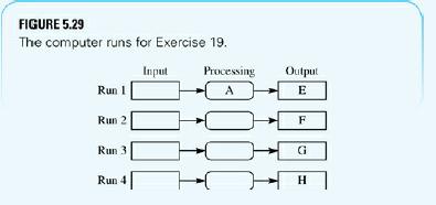
19. Assume you have a Pep/9-type computer and the following disk files:› File A: A Pep/9 assembly language assembler written in machine language› File B: A C-to-assembly-language compiler written in assembly language› File C: A C program that will read numbers from a data file and print their
16. Write the program in Figure 4.35 in hexadecimal format for input to the loader. Verify that it works correctly by running it on the Pep/9 simulator with an input of up. Then modify the store byte instruction at 0003 so that the first character is stored at Mem[FCAA] and the load byte
15. Write a machine language program to input two one-digit numbers, add them, and output the one-digit sum. There can be no space between the two one-digit numbers on input. Write the program in a format suitable for the loader and execute it on the Pep/9 simulator.
14. Write a machine language program to add the three numbers 2, –3, and 6 and output the sum on the output device. Store the –3 in hexadecimal. Do not use the subtract, negate, or invert instructions. Write the program in a format suitable for the loader and execute it on the Pep/9 simulator.
Showing 200 - 300
of 640
1
2
3
4
5
6
7
Step by Step Answers