

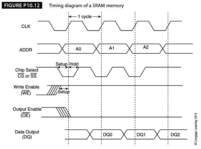
Given the timing diagram in Figure P10.12 that is derived from the data sheet of a commercial
Question:
Given the timing diagram in Figure P10.12 that is derived from the data sheet of a commercial SRAM, explain its action in words.
Fantastic news! We've Found the answer you've been seeking!
Step by Step Answer:
This is a read cycle because the write enable signal WE is inactivehigh i...View the full answer

Answered By
Joseph Mwaura
I have been teaching college students in various subjects for 9 years now. Besides, I have been tutoring online with several tutoring companies from 2010 to date. The 9 years of experience as a tutor has enabled me to develop multiple tutoring skills and see thousands of students excel in their education and in life after school which gives me much pleasure. I have assisted students in essay writing and in doing academic research and this has helped me be well versed with the various writing styles such as APA, MLA, Chicago/ Turabian, Harvard. I am always ready to handle work at any hour and in any way as students specify. In my tutoring journey, excellence has always been my guiding standard.
1+ Reviews
10+ Question Solved
Related Book For 

Computer Organization And Architecture Themes And Variations
ISBN: 9781111987046
1st Edition
Authors: Alan Clements
Question Posted:
