

Question: Ben Bitdiddle has invented a circuit with the transfer characteristics shown in Figure 1.47 that he would like to use as a buffer. Will it
Ben Bitdiddle has invented a circuit with the transfer characteristics shown in Figure 1.47 that he would like to use as a buffer. Will it work? Why or why not? He would like to advertise that it is compatible with LVCMOS and LVTTL logic. Can Ben’s buffer correctly receive inputs from those logic families? Can its output properly drive those logic families? Explain.
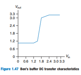
Vout 3.3 3.0 2.4 - 1.8 - 1.2 - 0.6 Vn 0- O 0.6 1.2 1.8 2.4 3.0 3.3 Figure 1.47 Ben's buffer DC transfer characteristics
Step by Step Solution
3.34 Rating (178 Votes )
There are 3 Steps involved in it
The circuit functions as a buffer with logic levels V IL 15 V I... View full answer

Get step-by-step solutions from verified subject matter experts