All Matches
Solution Library
Expert Answer
Textbooks
Search Textbook questions, tutors and Books
Oops, something went wrong!
Change your search query and then try again
Toggle navigation
FREE Trial
S
Books
FREE
Tutors
Study Help
Expert Questions
Accounting
General Management
Mathematics
Finance
Organizational Behaviour
Law
Physics
Operating System
Management Leadership
Sociology
Programming
Marketing
Database
Computer Network
Economics
Textbooks Solutions
Accounting
Managerial Accounting
Management Leadership
Cost Accounting
Statistics
Business Law
Corporate Finance
Finance
Economics
Auditing
Hire a Tutor
AI Study Help
New
Search
Search
Sign In
Register
study help
computer science
digital design computer
Questions and Answers of
Digital Design Computer
A supercomputer designer chooses to spend $1 million on DRAM and the same amount on hard disks for virtual memory. Using the prices from Figure 8.4, how much physical and virtual memory will the
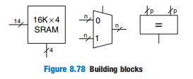
You are building a computer with a hierarchical memory system that consists of separate instruction and data caches followed by main memory. You are using the MIPS multicycle processor from Figure
You’ve joined a hot new Internet startup to build wrist watches with a built-in pager and Web browser. It uses an embedded processor with a multilevel cache scheme depicted in Figure 8.79. The
Write an HDL module implementing the days-in-month function from Question 2.2. Data from problem 2.2Write a Boolean equation in sum-of-products canonical form for each of the truth tables in Figure
If a computer uses 64-bit virtual addresses, how much virtual memory can it access? Note that 240 bytes = 1 terabyte, 250 bytes = 1 petabyte, and 260 bytes = 1 exabyte.
Repeat Exercise 8.16 with the following parameters.(a) The instruction cache is perfect (i.e., always hits) but the data cache has a 15% miss rate. On a cache miss, the processor stalls for 200 ns to
This chapter described the least recently used (LRU) replacement policy for multiway associative caches. Other, less common, replacement policies include first-in-first-out (FIFO) and random
Ben Bitdiddle and Alyssa P. Hacker are having another argument. Ben says, “I can get the two’s complement of a number by subtracting 1, then inverting all the bits of the result.” Alyssa says,
In a biased N-bit binary number system with bias B, positive and negative numbers are represented as their value plus the bias B. For example, for 5-bit numbers with a bias of 15, the number 0 is
Can addresses used for memory-mapped I/O be cached? Explain why or why not.
Explain how cache performance might be affected by the virtual page size of a memory system.
Explain the advantages and disadvantages of using a virtual memory system.
Explain how virtual memory systems work.
Explain the difference between direct mapped, set associative, and fully associative caches. For each cache type, describe an application for which that cache type will perform better than the other
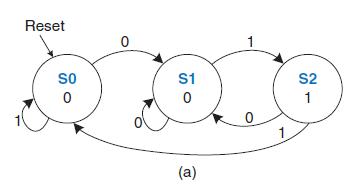
Repeat Exercise 8.29 for the FSM in Figure 3.30(a). The input A and output Y are memory-mapped to bits 0 and 1, respectively, of address 0xFFFFF040. Figure 3.30(a(a) Implement the traffic light
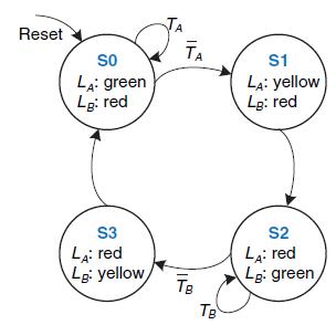
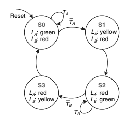
Finite state machines (FSMs), like the ones you built in Chapter 3, can also be implemented in software.(a) Implement the traffic light FSM from Figure 3.25 using MIPS assembly code. The inputs (TA
Use MIPS memory-mapped I/O to interact with a user. Each time the user presses a button, a pattern of your choice displays on five light-emitting diodes (LEDs). Suppose the input button is mapped to
Suppose you own a personal computer (PC) that uses 32-bit virtual addresses.(a) What is the maximum amount of virtual memory space each program can use?(b) How does the size of your PC’s hard drive
Describe a scenario in which the virtual memory system might affect how an application is written. Be sure to include a discussion of how the page size and physical memory size affect the performance
The virtual memory system you are designing uses a single-level page table built from dedicated hardware (SRAM and associated logic). It supports 25-bit virtual addresses, 22-bit physical addresses,
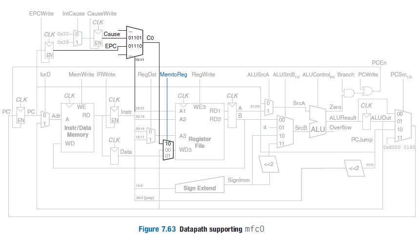
Suppose the MIPS multicycle processor described in Section 7.4 uses a virtual memory system.(a) Sketch the location of the TLB in the multicycle processor schematic.(b) Describe how adding a TLB
You decide to speed up the virtual memory system of Exercise 8.21 by using a translation lookaside buffer (TLB) with 128 entries.(a) How big (in bits) is the TLB? Give numbers for data (physical page
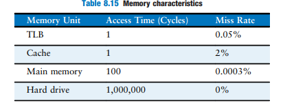
You decide to speed up the virtual memory system of Exercise 8.20 by using a translation lookaside buffer (TLB). Suppose your memory system has the characteristics shown in Table 8.15. The TLB and
Consider a virtual memory system that can address a total of 250 bytes. You have unlimited hard drive space, but are limited to 2 GB of semiconductor (physical) memory. Assume that virtual and
Consider a virtual memory system that can address a total of 232 bytes. You have unlimited hard drive space, but are limited to only 8 MB of semiconductor (physical) memory. Assume that virtual and
Consider a cache with the following parameters: N (associativity) = 2, b (block size) = 2 words, W (word size) = 32 bits, C (cache size) = 32 K words, A (address size) = 32 bits. You need consider
You are building an instruction cache for a MIPS processor. It has a total capacity of 4C = 2c+2 bytes. It is N = 2n -way set associative (N ≥ 8), with a block size of b = 2b′ bytes (b ≥ 8).
Suppose you are running a program with the following data access pattern. The pattern is executed only once.0x0 0x8 0x10 0x18 0x20 0x28 (a) If you use a direct mapped cache with a cache size of
Repeat Exercise 8.9 for the following repeating sequence of lw addresses (given in hexadecimal) and cache configurations. The cache capacity is still 16 words. 74 A0 78 38C AC 84 88 8C 7C 34 38
A 16-word cache has the parameters given in Exercise 8.8. Consider the following repeating sequence of lw addresses (given in hexadecimal): 40 44 48 4C 70 74 78 7C 80 84 88 8C 90 94 98 9C 0 4 8
A cache has the following parameters: b, block size given in numbers of words; S, number of sets; N, number of ways; and A, number of address bits.(a) In terms of the parameters described, what is
Each of the following statements pertains to the miss rate of caches. Mark each statement as true or false. Briefly explain your reasoning; present a counterexample if the statement is false.(a) A
Is the miss rate of a two-way set associative cache always, usually, occasionally, or never better than that of a direct mapped cache of the same capacity and block size? Explain.
Describe the trade-offs of increasing each of the following cache parameters while keeping the others the same:(a) Block size(b) Associativity(c) Cache size
Repeat Exercise 8.3 for the case when the fully associative cache outperforms the direct mapped cache. Data From Problem 3Come up with a sequence of addresses for which a direct mapped cache
Come up with a sequence of addresses for which a direct mapped cache with a size (capacity) of 16 words and block size of 4 words outperforms a fully associative cache with least recently used (LRU)
In one paragraph, describe two short computer applications that exhibit temporal and/or spatial locality. Describe how. Be specific.
In less than one page, describe four everyday activities that exhibit temporal or spatial locality. List two activities for each type of locality, and be specific.
Describe the concept of a superscalar processor and its pros and cons.
Describe what a hazard is in a microprocessor and explain ways in which it can be resolved. What are the pros and cons of each way?
If additional pipeline stages allow a processor to go faster, why don’t processors have 100 pipeline stages?
Explain the advantages of pipelined microprocessors.
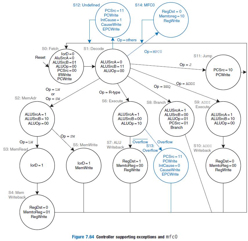
A nonmaskable interrupt (NMI) is triggered by an input pin to the processor. When the pin is asserted, the current instruction should finish, then the processor should set the Cause register to 0 and
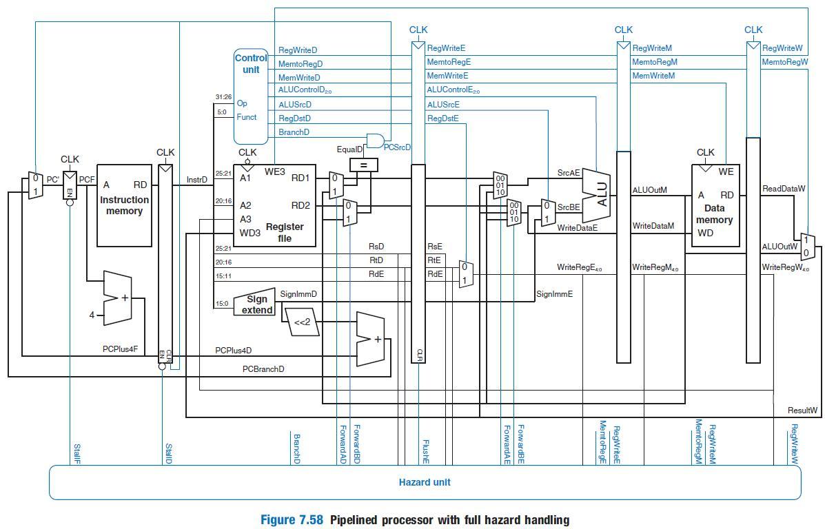
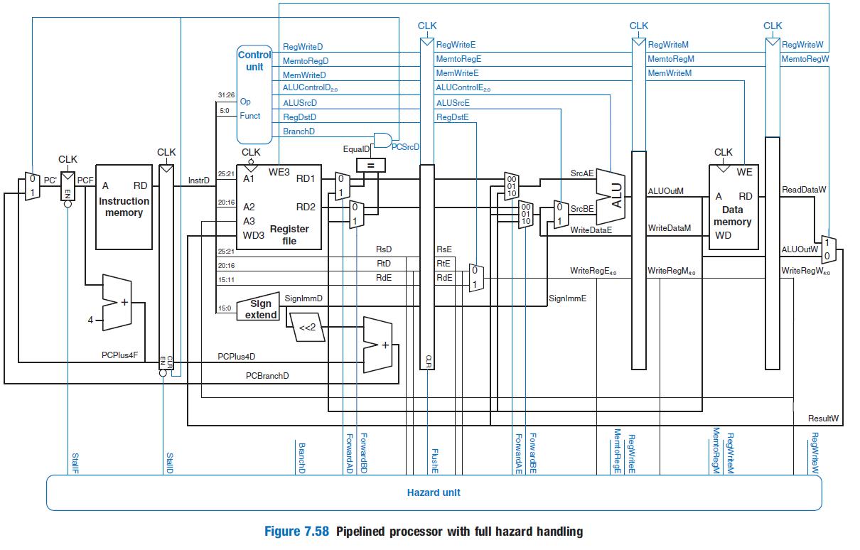
Design the hazard unit shown in Figure 7.58 for the pipelined MIPS processor. Use an HDL to implement your design. Sketch the hardware that a synthesis tool might generate from your HDL. CLK
Write HDL code for the pipelined MIPS processor. The processor should be compatible with the top-level module from HDL Example 7.13. It should support all of the instructions described in this
Suppose the MIPS pipelined processor is divided into 10 stages of 400 ps each, including sequencing overhead. Assume the instruction mix of Example 7.7. Also assume that 50% of the loads are
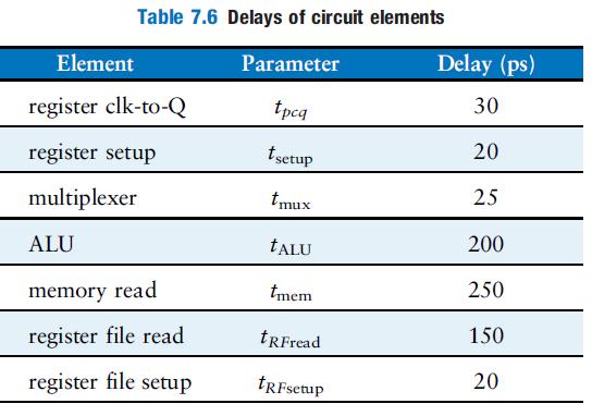
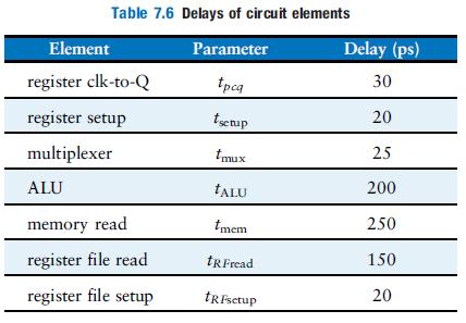
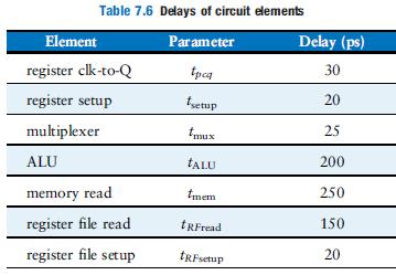
Consider the delays from Table 7.6 and Example 7.10. Now suppose that the ALU was 20% faster. Would the cycle time of the pipelined MIPS processor change? What if the ALU were 20% slower? Table
Your friend, the crack circuit designer, has offered to redesign one of the units in the pipelined MIPS processor to be much faster. Using the delays from Table 7.6 and Example 7.10, which unit
Examples 7.9 and 7.10 point out that the pipelined MIPS processor performance might be better if branches take place during the Execute stage rather than the Decode stage. Show how to modify the
Explain how to extend the pipelined processor to handle the j instruction. Give particular attention to how the pipeline is flushed when a jump takes place.
Explain how to extend the pipelined MIPS processor to handle the addi instruction.
Repeat Exercise 7.32 for the instructions of the program in Exercise 7.24.
How many cycles are required for the pipelined MIPS processor to issue all of the instructions for the program in Exercise 7.23? What is the CPI of the processor on this program?? Data from Problem
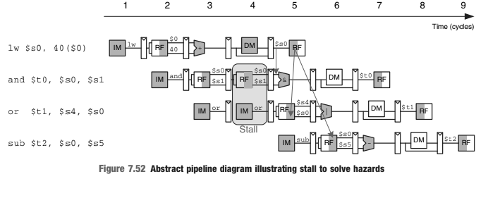
Repeat Exercise 7.30 for the following instructions.? Data From Problem 30 Using a diagram similar to Figure 7.52, show the forwarding and stalls needed to execute the following instructions on the
Using a diagram similar to Figure 7.52, show the forwarding and stalls needed to execute the following instructions on the pipelined MIPS processor.? add $t0, $s0, $s1 sub $t0, $t0, $s2 $t1, 60(
Repeat Exercise 7.28 for the following MIPS program. Recall that the pipelined MIPS processor has a hazard unit.? Data from Problem 28 The pipelined MIPS processor is running the following program.
The pipelined MIPS processor is running the following program. Which registers are being written, and which are being read on the fifth cycle?? addi $s1, $s2. 5 sub $t0, $t1, $t2 1w $t3, 15 ( $s1)
Repeat Exercise 7.26 for one of the new instructions from Exercise 7.14.
Extend your HDL code for the multicycle MIPS processor from Exercise 7.25 to handle one of the new instructions from Exercise 7.13. Enhance the testbench to test the new instruction.
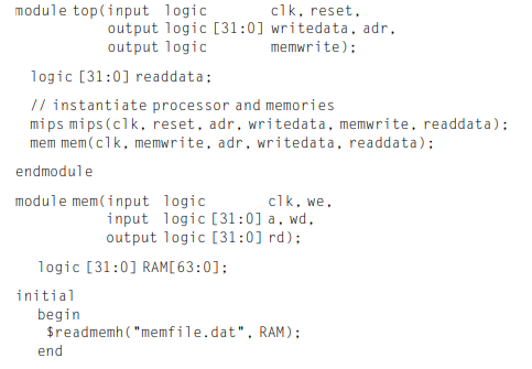
Write HDL code for the multicycle MIPS processor. The processor should be compatible with the following top-level module. The mem module is used to hold both instructions and data. Test your
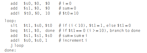
Repeat Exercise 7.23 for the following program. Data From Problem 23 How many cycles are required to run the following program on the multicycle MIPS processor? What is the CPI of this program??
How many cycles are required to run the following program on the multicycle MIPS processor? What is the CPI of this program?? addi $s0, $0, done # result = 5 while: beq $s0, $0, done # if result >
What is the CPI of the redesigned multicycle MIPS processor from Exercise 7.21? Use the instruction mix from Example 7.7.
Goliath Corp claims to have a patent on a three-ported register file. Rather than fighting Goliath in court, Ben Bitdiddle designs a new register file that has only a single read/write port (like the
Suppose the multicycle MIPS processor has the component delays given in Table 7.6. Alyssa P. Hacker designs a new register file that has 40% less power but twice as much delay. Should she switch to
Repeat Exercise 7.8 for the multicycle processor. Assume the instruction mix of Example 7.7.
Your friend, the crack circuit designer, has offered to redesign one of the units in the multicycle MIPS processor to be much faster. Using the delays from Table 7.6, which unit should she work on to
Suppose that the floating-point adder and multiplier from Exercise 7.16 each take two cycles to operate. In other words, the inputs are applied at the beginning of one cycle, and the output is
Repeat Exercise 7.6 for the multicycle MIPS processor. Data From Problem 6Add a single-precision floating-point unit to the single-cycle MIPS processor to handle add.s, sub.s, and mul.s. Assume
Repeat Exercise 7.5 for the multicycle MIPS processor. Show the changes to the multicycle datapath and control FSM. Is it possible to add the instruction without modifying the register file?
Repeat Exercise 7.13 for the following MIPS instructions.(a) bne(b) lb(c) lbu(d) andi? Data from problem 3 Modify the single-cycle MIPS processor to implement one of the following instructions. See
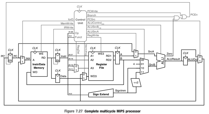
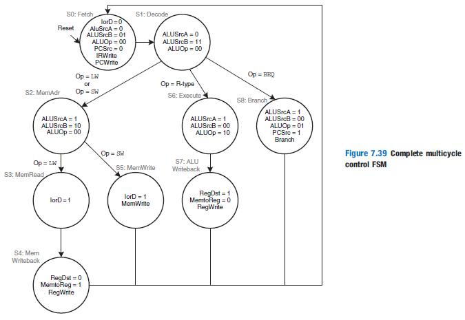
Modify the multicycle MIPS processor to implement one of the following instructions. See Appendix B for a definition of the instructions. Mark up a copy of Figure 7.27 to indicate the changes to the
Repeat Exercise 7.11 for the new instructions from Exercise 7.4.
Modify the HDL code for the single-cycle MIPS processor, given in Section 7.6.1, to handle one of the new instructions from Exercise 7.3. Enhance the testbench, given in Section 7.6.3, to test the
Repeat Exercise 7.9, assuming that the signal has a stuck-at-1 fault. Data from Problem 9Suppose one of the following control signals in the multicycle MIPS processor has a stuck-at-0 fault,
Suppose one of the following control signals in the multicycle MIPS processor has a stuck-at-0 fault, meaning that the signal is always 0, regardless of its intended value. What instructions would
Consider the delays given in Table 7.6. Ben Bitdiddle builds a prefix adder that reduces the ALU delay by 20 ps. If the other element delays stay the same, find the new cycle time of the single-cycle
Your friend is a crack circuit designer. She has offered to redesign one of the units in the single-cycle MIPS processor to have half the delay. Using the delays from Table 7.6, which unit should she
Add a single-precision floating-point unit to the single-cycle MIPS processor to handle add.s, sub.s, and mul.s. Assume that you have singleprecision floating-point adder and multiplier units
Many processor architectures have a load with post-increment instIt is not possible to implement this instruction without either modifying the register file (adding another write port) or making the
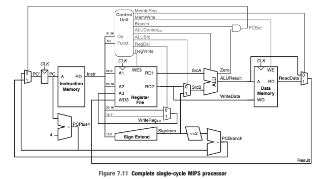
Modify the single-cycle MIPS processor to implement one of the following instructions. See Appendix B for a definition of the instructions. Mark up a copy of Figure 7.11 to indicate the changes to
Repeat Exercise 7.1, assuming that the signal has a stuck-at-1 fault. Data from problem 1Suppose that one of the following control signals in the single-cycle MIPS processor has a stuck-at-0
Suppose that one of the following control signals in the single-cycle MIPS processor has a stuck-at-0 fault, meaning that the signal is always 0, regardless of its intended value. What instructions
Design an algorithm for testing whether a given string is a palindrome. (Recall that a palindrome is a word that is the same forward and backward. For example, the words “wow” and “racecar”
Write MIPS assembly code to test whether overflow occurs when $t2 and $t3 are added. Use a minimum number of instructions.
Write MIPS assembly code to reverse the bits in a register. Use as few instructions as possible. Assume the register of interest is $t3.
Design an algorithm for counting the number of 1’s in a 32-bit number. Implement your algorithm using MIPS assembly code.
You are given an array that holds a C string. The string forms a sentence. Design an algorithm for reversing the words in the sentence and storing the new sentence back in the array. Implement your
2 Suppose you are given an array of both positive and negative integers. Write MIPS assembly code that finds the subset of the array with the largest sum. Assume that the array’s base address and
Write MIPS assembly code for swapping the contents of two registers, $t0 and $t1. You may not use any other registers.
Exercise 6.39 Repeat Exercise 6.38 for the following pseudoinstructions. (a) beq $t1, imm31:0, L(b) ble $t3, $t5, L(c) bgt $t3, $t5, L(d) bge $t3, $t5, L Data from Problem 38Show the MIPS
Show the MIPS instructions that implement the following pseudo instructions. You may use the assembler register, $at, but you may not corrupt (overwrite) any other registers. (a) addi $t0, $s2,
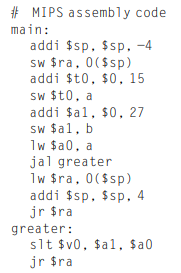
Repeat Exercise 6.36 for the following MIPS code.? # MIPS assembly code main: addi $sp, $sp, -4 sw $ra, 0($sp) addi $t0, $0, 15 Sw $t0, a addi $al, $0, 27 sw $al, b 1w $a0, a jal greater 1w $ra,
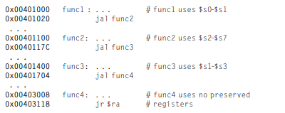
Consider the MIPS assembly code below. func1, func2, and func3 are non-leaf functions. func4 is a leaf function. The code is not shown for each function, but the comments indicate which registers are
Show how the following MIPS program would be loaded into memory and executed.
Write a MIPS assembly program that adds two positive singleprecision floating point numbers held in $s0 and $s1. Do not use any of the MIPS floating-point instructions. You need not worry about any
Consider two strings: string1 and string2.(a) Write high-level code for a function called concat that concatenates (joins together) the two strings: void concat(char string1[], char string2[], char
Write a function in high-level code that takes a 10-entry array of 32-bit integers stored in little-endian format and converts it to big-endian format. After writing the high-level code, convert it
Write assembly code that jumps to an instruction 64 Minstructions from the first instruction. Recall that 1 Minstruction = 220 instructions = 1,048,576 instructions. Assume that your code
Explain why it is advantageous to have a large address field, addr, in the machine format for the jump instructions, j and jal.
Showing 1 - 100
of 430
1
2
3
4
5