

Question: Write and verify the VHDL for the SOS flasher (datapath + microcoded FSM) of Exercise 18.7. Data in Exercise 18.7. Modify the microcoded FSM and
Write and verify the VHDL for the SOS flasher (datapath + microcoded FSM) of Exercise 18.7.
Data in Exercise 18.7.
Modify the microcoded FSM and microcode from Section 18.1 and Exercise 18.6 to act as a control module to interface with a datapath of your design. Provide a block diagram of this datapath, the signals needed to interface between the two, and your microcode.
Data in Section 18.1
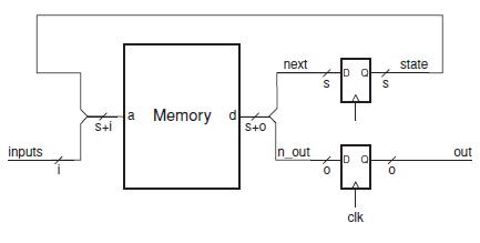
Figure 18.1 shows a block diagram of a simple microcoded FSM. A memory array holds the next-state and output functions. Each word of the array holds the next state and output for a particular combination of input and current state. The array is addressed by the concatenation of the current state and the inputs. A pair of registers holds the current state and current output. In practice, the memory could be realized as a RAM or EEPROM allowing software to reprogram the microcode. Alternatively, the memory could be a ROM. With a ROM, a new mask set is required to reprogram the microcode. However, this is still advantageous because changing the program of the ROM does not otherwise alter the layout of the chip. Some ROM designs even allow the program to be changed by altering only a single metal-level mask – reducing the cost of the change. Some designs take a hybrid approach, putting most of the microcode into ROM (to reduce cost) but keeping a small portion of microcode in RAM. A method is provided to redirect an arbitrary state sequence into the RAM portion of the microcode to allow any state to be patched using the RAM.
Data in Figure 18.1
Data in Exercise 18.6
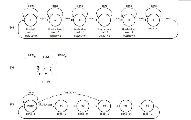
Write the microcode for an SOS flasher (Exercise 17.11). While the input flash is high, your system should flash an SOS sequence – three short flashes (one clock each) followed by three long flashes (four clocks each) followed by three short flashes again. Spaces within each character should be one clock long. Spaces between characters within one SOS should be three clocks long. Spaces between one SOS and the next SOS should be seven clocks long. When the input is lowered, the flasher should reset back to a reset state. Use the microcoded FSM of Section 18.1. Leave your flasher completely unfactored.
Data in Exercise 17.11
Modify the flasher FSM of Figure 17.2 to flash an SOS sequence – three short flashes (one clock each), followed by three long flashes (four clocks each),followed by three short flashes again. Spaces within each character should be one clock long. Spaces between characters within one SOS should be three clocks long. Spaces between one SOS and the next SOS should be seven clocks long.
Data in Figure 17.2
Step by Step Solution
3.36 Rating (159 Votes )
There are 3 Steps involved in it
To design the SOS flasher we need to first design a datapath and then design the microcoded FSM to interface with the datapath Datapath Design The dat... View full answer

Get step-by-step solutions from verified subject matter experts