

Question: Using the following components: 4-bit general-purpose register, 4-bit adder/ subtractor, and tristate buffer, and assuming the inbus and outbus are 4 bits wide, design a
Using the following components: 4-bit general-purpose register, 4-bit adder/ subtractor, and tristate buffer, and assuming the inbus and outbus are 4 bits wide, design a control unit using hardwired control to perform the operations shown in Figure P6.13. You may use counters, decoders, and PLAs as required.
(a) Outbus ← 4 A. Assume A is a 4-bit unsigned number and the result is 4 bits wide.
(b) If the 4-bit number in register B is odd, outbus ← 0; otherwise outbus ← A + (B/2). Assume A and B are unsigned 4 bit numbers. Also, assume data is already loaded into B.
(c) If the content of a 4-bit register Q = 0, perform R ← M and then transfer the 4-bit result to outbus. On the other hand, if the content of the 4-bit register Q = 0, perform R ← 0 and then transfer the 4-bit result to the outbus. Assume M and R are 4 bits wide.
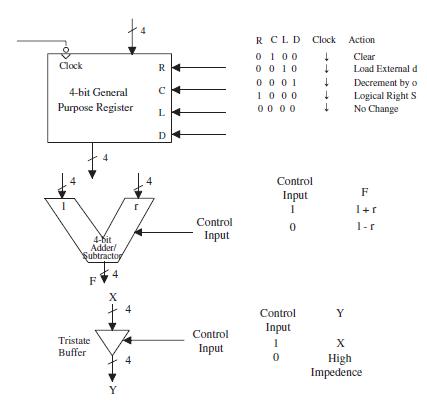
Clock 4-bit General Purpose Register 4-bit Adder/ Subtractor F Tristate Buffer X Y R L D Control Input Control Input R CLD Clock Action Clear Load External d 0100 0 0 10 0001 1000 0000 Control Input 1 0 Control Input 1 0 Y Decrement by o Logical Right S No Change F 1 + r 1-r X High Impedence
Step by Step Solution
3.38 Rating (167 Votes )
There are 3 Steps involved in it
a Step1 Step 2 Step 3 Components are specified in the problem Step 4 ... View full answer

Get step-by-step solutions from verified subject matter experts