

Question: Write a Verilog description using behavioral modeling for: (a) The positive edge-triggered JK Flip-Flop of Figure 5.9. (b) A D flip-flop with a synchronous reset
Write a Verilog description using behavioral modeling for:
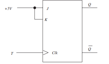
(a) The positive edge-triggered JK Flip-Flop of Figure 5.9.
(b) A D flip-flop with a synchronous reset input and a positive edge triggered clock. Use synchronous reset such that if reset ==0, the flip-flop is cleared to 0; on the other hand, if reset==1, the output of the flip-flop is unchanged until the procedural statements are evaluated at the positive edge of the clock.
(c) The T flip-flop of Figure 5.10(b).
(d) The T flip-flop of Problem 5.13(b) with a HIGH reset input.
(e) The state machine of Problem 5.19.
(f) A 4-bit binary ripple counter. Note that in a binary ripple counter, the clock inputs of high order flip-flops are not triggered by the common clock, but by the transition outputs of the low order flip-flops. The 4-bit binary ripple counter contains four T flip-flops (obtained from D-ffs), with the output of each ff connected to the clock input of the next higher-order ff. The clock input is connected to the least significant T-ff. The 4-bit ripple counter can be designed using four T flip- flops (tff0 through tff3). Each T-ff can be obtained from a D-ff by connecting its output q to the input of an inverter, and then connecting the inverter output to the D input; the T-ff has one input (T input is the same as the clock input). This T-ff toggles every clock. The 4-bit ripple counter can be obtained by connecting the clock to the tff0 clock input, q0 of tff0 to clock input of tff1, q1 output of tff1 to clock input of tff2, and q2 output of tff2 to the clock input of tff3. Use negative edge-triggered D-ffs. Each D-ff will have a reset input to clear the ff.
(g) A 4-bit serial shift (right) register with a positive edge triggered reset and a positive edge triggered clock. The 4-bit serial shift register can be obtained by connecting four D-ff’s to a common clock and a common reset. The four D-ff’s are cleared to 0 at the positive edge triggered clock and positive edge triggered reset. Assume, v as the serial input bit connected to the D input of the left-most D-ff with z as its output; z is connected to the D input of the next right D-ff with y as its output; y is connected to the D input of the next right D-ff with x as its output; finally, x is connected to the D input of the right-most D-ff with w as its output.
(h) A 4-bit register with a reset input, a parallel load input and a positive edge-triggered clock. The 4-bit register is cleared to 0 at the positive edge of the reset. On the other hand, if the load input is high, 4-bit data is transferred to the register at the positive edge of the clock. Use behavioral modeling.
(i) The counters of Problems 5.24 (a) through 5.24 (c).
(j) The general purpose register of Problem 5.25.
+5V T K Clk Q Q
Step by Step Solution
3.48 Rating (158 Votes )
There are 3 Steps involved in it
a Positive edgetriggered JK b Dff with reset and positive edge triggered clock c T ... View full answer

Get step-by-step solutions from verified subject matter experts